![Gallery[1762]](http://images.twibright.com/tns/lvl2/1762.jpg)
Ask on the Mailing list and I'll add the question and answer here.
The photodiode has a rather high bias voltage of 12V. It's not much considering the maximum allowed voltage 50V (SFH203). This guarantees that the carrier-free region in junction is wide and the capacitance small.
The receiver circuit works in a way, that the smaller the capacitance of the diode (+ input capacitance of Q101), the higher signal is received.
The photodiode has intentionally high working (load) resistance in order of hundred kiloohm to achieve low-noise operation. This totally destroys the bandwidth - it actually starts to work as an interator with single-pole slope of 6dB/octave.
Leaving the bandwidth "conventionally" as should be would reqire working resistance of about 3 kOhm. Johnson noise of the resistor destroys the noise performance of the receiver totally - the on-floor range goes down to about 1/3, according to a rough experiment performed.
The deformed spectral response is later straightened out by NE592 acting as a derivator.
The MOSFET internally works as a cascode. The Q101 transistor is basically a silicon version of tetrode tube. G2 voltage regulates the operating voltage of lower half of the tetrode/cascode and this influences gain of the lower half. The upper half just prevents Miller effect to take place, which reduces the feedback capacitance drastically. Feedback capacitance would otherwise decrease the voltage gain.
We are having the gain at maximum by putting G2 to maximum allowed voltage. The working resistor of Q101 must be possible to replace because drain current varies very much piece to piece (and also type to type).
NE592 acts as a derivator and amplifier in one. It's gain is set to maximum and 270pF capacitor defines upper cutoff frequency at about 17MHz.
NE592's differential output is used as two independent sources of signal. One source is for driving the cable and the other is detected and used as a measurement of signal strength
A voltage doubler is used. It generates DC voltage from AC value. The response of the doubler is frequency dependent. Therefore the DC voltage during packet with the same signal strength is smaller than DC voltage during 1MHz stuffing wave.
Schottky diodes in the doubler are used for their low voltage drop and high switching speed.
RSSI cannot be taken as absolute value. It differs very remarkably from piece to piece. Q101 gain and Q101 operating current determine RSSI behaviour. Also it's very nonlinear, caused by characteristics of the Schottky diodes. At low signal levels, Q101 noise or shot noise from ambient lighting is received. Therefore minimum value of RSSI may not be zero. RSSI levels also may wander substantially with temperature due to change in diode jusction properties and conductivity of Q101.
For these low guarantee about RSSI properties, RSSI may be used only for alignment (finding of maximum) or monitoring purposes. Monotonicity of RSSI is guaranteed if overdrive of NE592 doesn't occur. Overdrive occurs at about 4V of RSSI.
End stage is a differential limiting amplifier made of two bipolar transitors, Q102 and Q103. Collector of the Q103 transistor acts as a current cource working into 75 Ohm resistor. This way output impedance of 75 Ohm is guranteed independently of switching state of the output stage.
The input of NE592 is differential. Both branches see the same crappiness, therefore it will cancel out. The purpose of P105 is just to provide a reasonable floating ground with moderate immunity to load by signal.
The leak current of NE592 input doesn't shift the level at P105 substantially.
C161 programs NE592 frequency response and gain. See datasheet, "FILTER NETWORKS"
R114 prevents overload of pin7 of U101. If it's overloaded (as was in case when R114 used to be only 100 Ohm), the output staget of U101 distorts it's signal and the distortion propagates also to pin 8 (the other half of the differential output) where the useful signal is damaged and range reduced.
A bug has been found in the RX (radiation of the packet about 10mVpp) which will mean changes in the schematic. First problem was 220nF blocking the 700mV signal over 75 Ohm cable impedance to ground was too small for 1MHz frequency. It was increased to 22uF - this value was computed to get theoretically to 100uV at 1MHz.
After placing 22uF it showed that the lead length of 22uF are inductance problem. The big glue drop holding the cable was standing in a way so the mechanic construction was changed: a tin tube was added which is to be filled with glue. Then there is actually no glue inside the RX case and capacitors can be placed with leads directly to the cable.
|
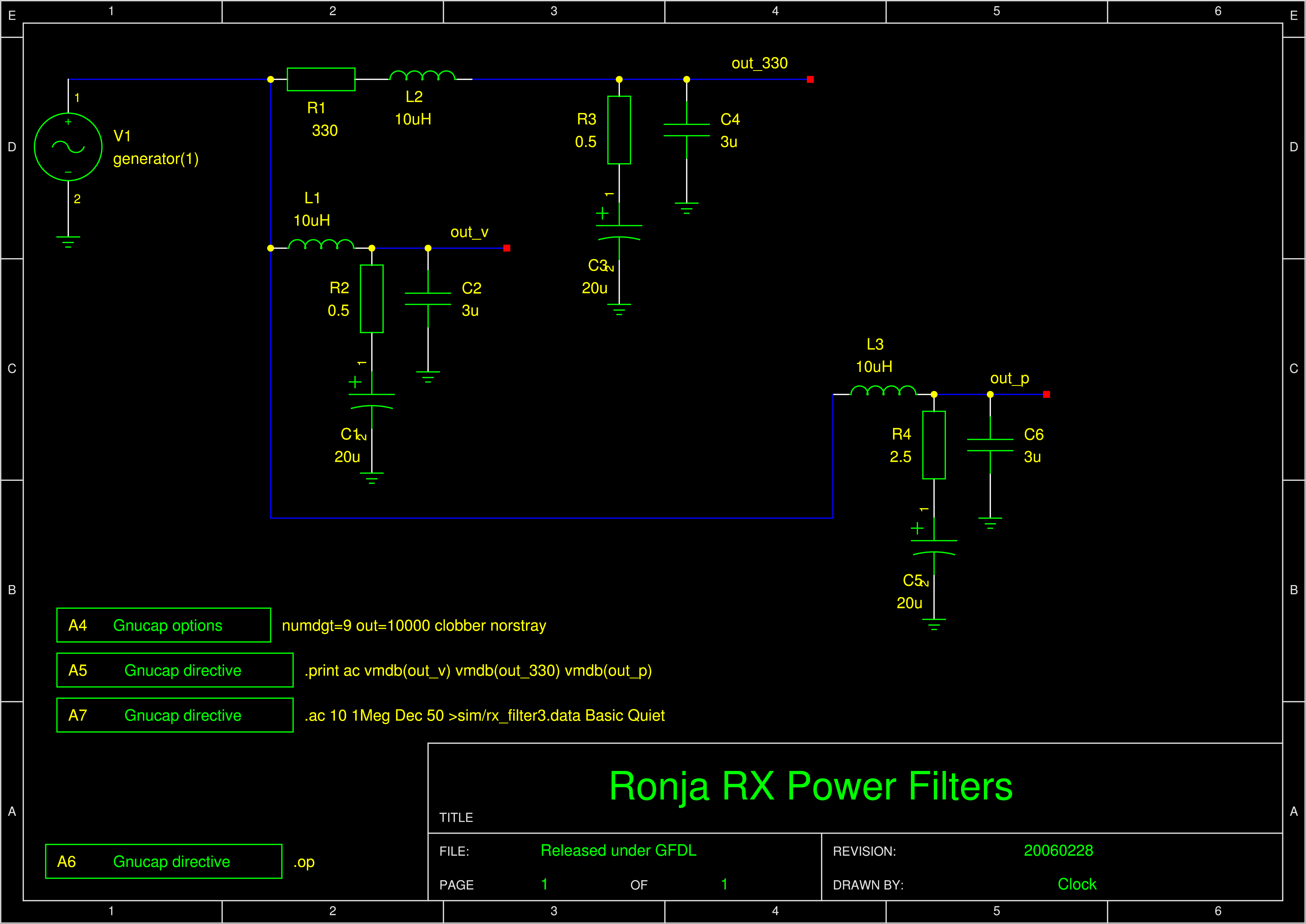
First (bad) filterA power filter was designed with 22uF capacitor but a resonance problem showed in the theoretical analysis which was amplifying garbage in order of kHz several times (like 4x or 6x). Damping resistors R1 and R2 were added and resonance got down to about 1.2x amplification. However real performance of this filter on oscilloscope was horrible - 6mV of 1MHz on the cable shield. Measurement revealed there is 1mVpp triangle wave 1MHz on the internal point in RX before the filter. Therefore the filter passing was not source of the problem. Source therefore must have been parasitic inductance of axial 22uF capacitor. Another problem is 0.68 Ohm in parallel with the coil - the filtration at high frequencies won't be good due to parasitic resistance of capacitors. | |||||||||||||||||||||||||||||||||||
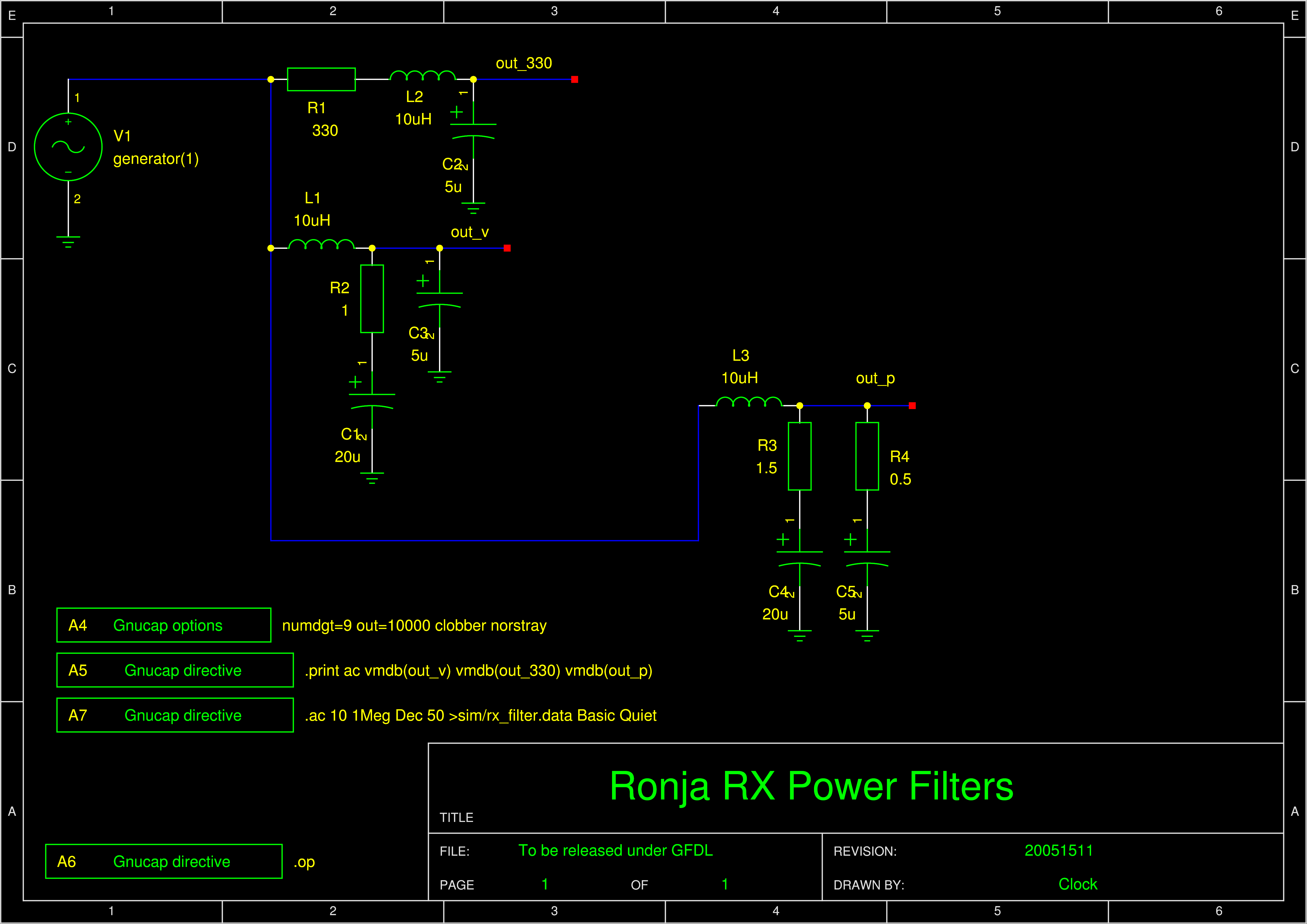
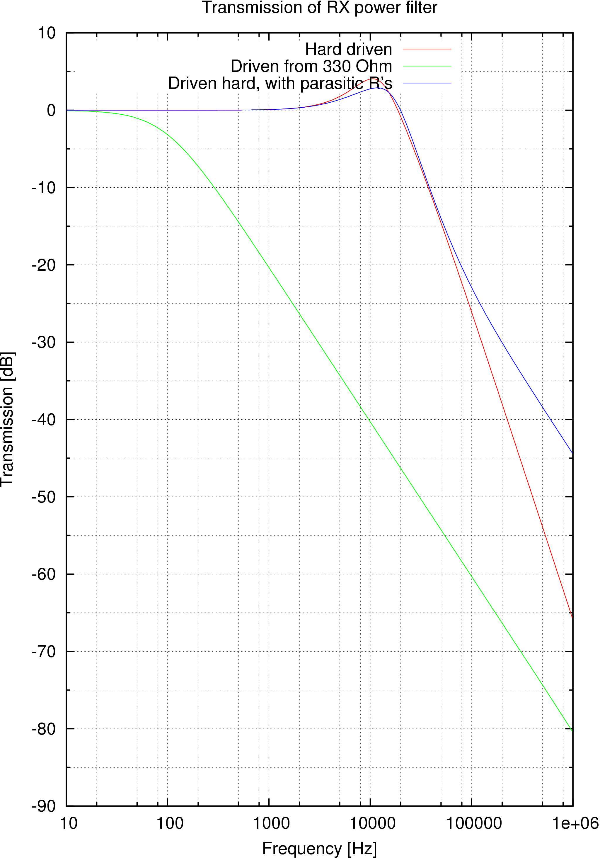
| Value of C2 (22u) was decided to be decreased to not get so low damping resistances. Target of 300uV at 1MHz for 75Ohm and 700mV was set which leads to 5uF. 5uF with 10uH have critical damping at 8 Ohm and resonance at 22.5kHz. Parasitic resistance of the capacitors was assumed to be max. 0.5 Ohm and parasitic inductance max. 5nH. Coil parallel resistance was removed this time altogether and Boucherot damping cell from 100uF capacitor and resistor was employed. The resistor was optimized for minimum resonance peak of about 1.1 at value of 1Ohm. | |||||||||||||||||||||||||||||||||||
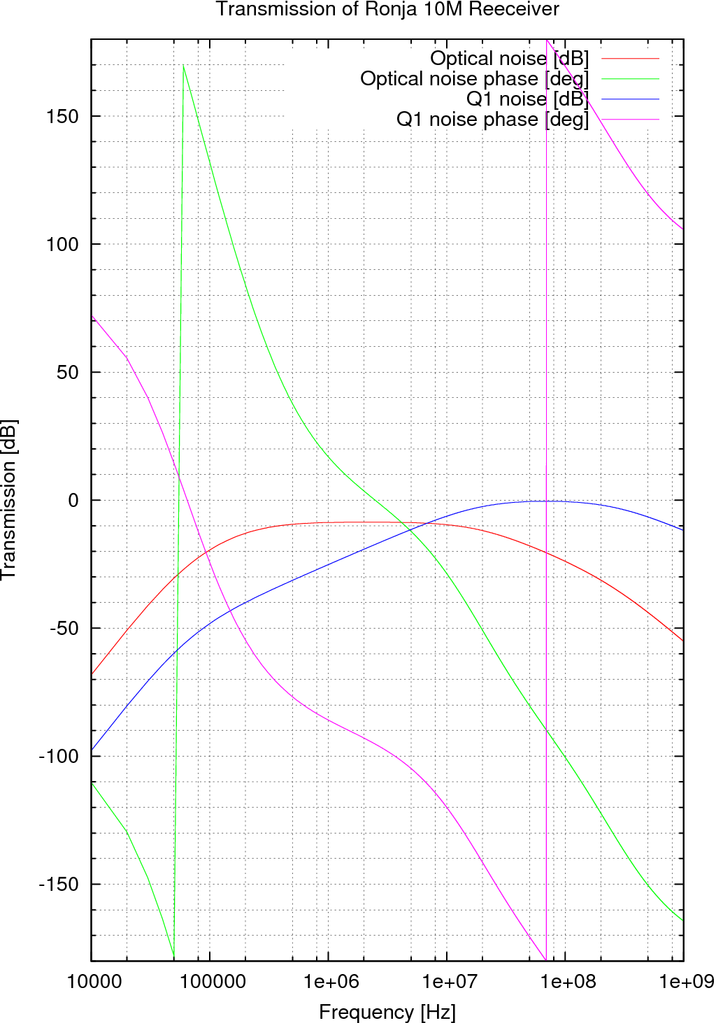
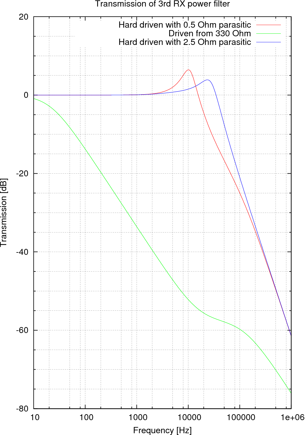
| Here you can see transmission characteristics of the filter driven hard, driven by 330 Ohm and driven hard with capacitor parasitic resistances of 0.5 Ohm. |
1mVpp was set as a goal for reduction of the cable shield noise as it seems to be a difficult task to get rid of it. To attenuate 750mV at 75 Ohm down to 1mV, 1.6uF capacitor is needed. We therefore chose a triplet of 1uF ceramic capacitors. 1uF because 2.2uF seem to be hard to get, 1uF seems to be the last value that is widely available. 3 of them because they have crappy dielectric with large tolerance and to have some reserve for ESR and lead inductance effects. 3 pieces are also good because it cuts down ESR 3 times and lead inductance 3 times. However, it won't change the resonance frequency.
We also removed the damping resistor because now we suspect that the internal ESR of electrolytic capacitors will be enough to damp possible oscillations at low frequency.
| |||||||||||||||||||||||||||||||
| |||||||||||||||||||||||||||||||
| |||||||||||||||||||||||||||||||
We put 3 capacitors into the RX as close to the hole where the shielded cable is leaving the shielding enclosure. We put also 3 capacitors in parallel inside the shielding enclosure of Twister, as close as possible to the hole where the wire for cable shield (12V for optical heads) is leaving the Twister shielding enclosure. We measured at 1MHz, 5MHz and 10MHz with oscilloscpe bandwidth set to 20MHz.
At 1MHz the noise has shape of triangle wave with notches. The triangle wave has peak-to-peak amplitude something below 1mV. There are two kinds of notches. Big notches 60ns after the wave breaks of amplitude 700uV, and small notches 56ns before the wave breaks of amplitude 520uV. The big notches point inwards into the wave so they don't increase the peak voltage and the small ones outward, so they increase. slightly. The voltage indicated is without the notches. The duration of both notches is 40ns.
At 5Mhz there are LF damped oscillations with period of 6us and biggest difference between successive peaks 6mV, repeated every 236us. The 5Mhz signal superimposed is with shape of square wave with overshoot after every edge. The square wave pp is about 250uV. The pp with overshoots is 1.2mV. The overshoot duration is about 20ns and both overshoots (leading and trailing) are symmetrical.
At 10Mhz the signal is a deformed triangle wave with 1.7mV pp and 700uV 6.4ns 500uV downward peak in the middle.
The RSSI during measurement was 3.6V. The receiver was with BC547C and uA733 TO-5-10.
We then measured with the TX power internally disconnected to remove the interference generated by RX and see only interference generated by Twister. The result: A noise ringing with period 31.25ns is present on CONN53-4. 31.25 is the period of 16MHz clock frequency edge transitions. The frequency of the ringing is 200MHz and largest step observed (distance between successive peak and valley) is 10mV. This remains even when the RX and TX modules have internally disconnected power and the middle of the coaxial cable leading to RX (CONN53-3) is disconnected at the Twister's terminal block. The apparent noise size is highly sensitive to scope bandwidth which supports the finding that it is not a broadband noise: Measurement with no input from network card. The Twister enclosure was closed only on 2 screws instead of 10.
| Shielding boxes open | Bandwidth | Modules with internally disconnected power | Noise between RX's J101 and J102 (measured outside) |
|---|---|---|---|
| - | 20MHz | TX | 360uV alternating spikes in rhythm of 1MHz 30ns long |
| - | 150MHz | TX | 6mVpp noise |
| - | 300MHz | TX | 10mVpp noise |
| RX | 20MHz | RX, TX | 360uV alternating spikes in rhythm of 1MHz 30ns long |
| RX | 150MHz | RX, TX | 7mVpp noise |
| RX | 300MHz | RX, TX | 12mVpp noise |
Then we added 47nH in series with the 12V wire of CONN53-4 with this result:
| Shielding boxes open | Bandwidth | Modules with internally disconnected power | Noise between RX's J101 and J102 (measured outside) |
|---|---|---|---|
| - | 20MHz | TX | 380uV alternating spikes in rhythm of 1MHz 30ns long |
| - | 150MHz | TX | 4.5mVpp noise |
| - | 300MHz | TX | 8.96mVpp noise |
| RX | 20MHz | RX, TX | 320uV alternating spikes in rhythm of 1MHz 30ns long |
| RX | 150MHz | RX, TX | 6.18mVpp noise |
| RX | 300MHz | RX, TX | 8.8mVpp noise |
I removed the CONN53-4 from inside the Twister box so that the shield of the coaxial connected to 4 ceramic capacitors to the ground only (and 47nH coil with one end floating). With Twister shielding open and RX and TX shielding closed and TX power internally disconnected it makes 6.28mVpp @300MHz BW.
Then I closed the shield and the peak-to-peak value rised to 10.7mV. That suggests the interference is not on CONN53-4, but on the ground and the ground is propped against interference leaked by other wire - DC supply or ethernet cable.
I disconnected the TP cable inside and removed the shield. The level is now 8.64mV. Im closing the shield and the level stays - now it reads 8.4mV. The prime suspect is now the power cable. It actually doesn't have any series coil at all!
I added another 47nH in series with the power supply wire at the power supply connector and the situation hasn't changed.
Then I started to suspect the shielding box. I soldered up the box to make sure the contact is perfect on multiple places. Nothing changed. Then I disconnected the RX and TX blue inner wires from the terminal block (on outside of the shielding enclosure) and the interference ceased. Totally.
When I touch a screwdriver to the signal wires it starts making noise a bit. When I connect a longer wire it makes a lot of noise. The problem is in the fact that the shielding is not perfectly continuous. Between the shielding enclosure and the place where the shielded cable is stripped there is about 5 cm of unshielded cable. And that's the problem.
The proposed solution is to make the shield of the whole system tightly closed, without any gaps or slots. The terminal blocks will be changed to DE9 connectors and the shielding box will be soldered directly to the PCB. The lids will not be closed by screws becasuse:
The lids will be attached by soldering along the edge, on a corner joint. Opening will be done by standing the box vertically, melting one end, prying a small screwdriver into the slit and moving it along with the soldering iron to unsolder the joint along the whole length. Natural flexibility of the lid will be taken advantage of. Here is a prototype template:
Warning: fopen(../drawings/prototype.php): failed to open stream: No such file or directory in /home/clock/www/twibright.com/ronja/boxed_page.php on line 103 Warning: filesize(): stat failed for ../drawings/prototype.php in /home/clock/www/twibright.com/ronja/boxed_page.php on line 104 Warning: fread() expects parameter 1 to be resource, boolean given in /home/clock/www/twibright.com/ronja/boxed_page.php on line 104 Warning: fclose() expects parameter 1 to be resource, boolean given in /home/clock/www/twibright.com/ronja/boxed_page.php on line 105The experimental RX has a supply rail that feeds all the bases of the current sources. This is filtered to prevent feedback and resulting oscillations or signal distortion.
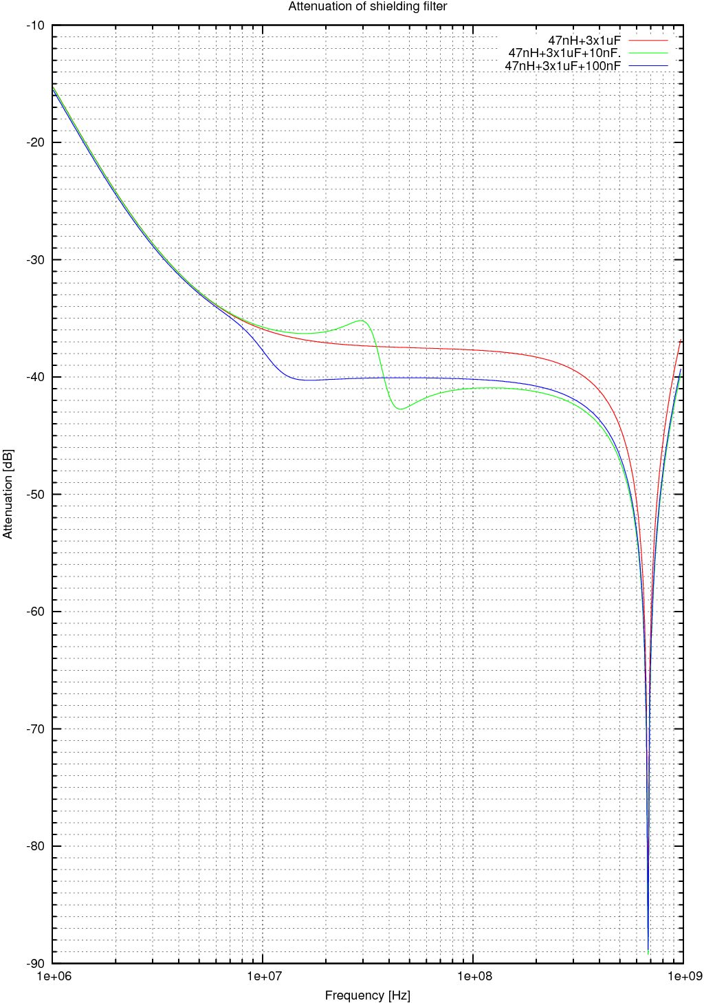
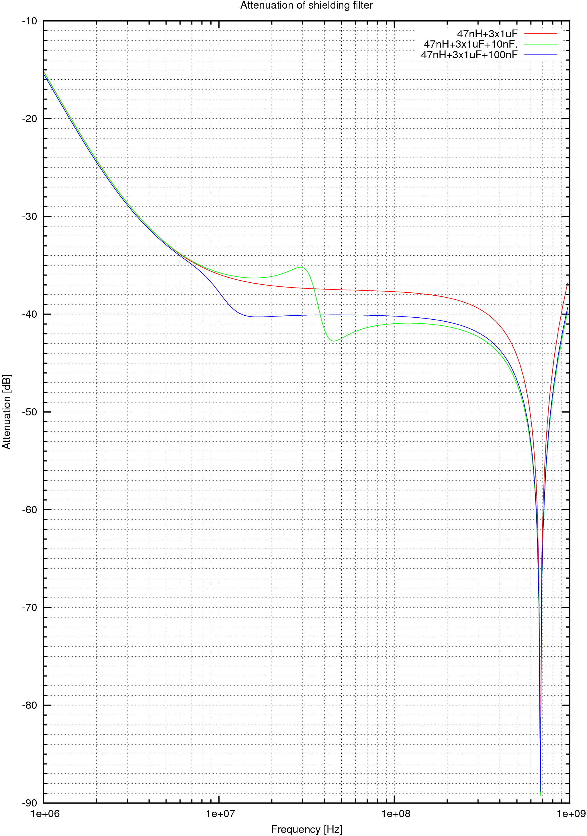
First a combination of 47nH and 100nF was calculated with a coil bypass resistor to dampen oscillations. That yielded optimum resistance of 1.2 Ohm, which is probably too low for the internal resistance of the capacitors.
Next the inductance was increased to 1uH. The criterium was set to minimize the worst attenuation from 100kHz upwards. That was best for 8.2 Ohm resistor with -46dB. Let's consider this enough to overcome the unknown internal resistance of the ceramic capacitors.
A new design of Twister, called Twister2 was designed because of the interference issues. Everything was enclosed as tightly as possible and DE9 connectors, which are somehow shielded, have a reliable contact and contacts spaced closely together, were chosen. The shield was continuously connected to the ground plane, which created a space issue for the regulator. Therefore the heating linear regulator was replaced with a switched one which doesn't heat.
The case of the prototype was slightly modified. Corners were improved and the lid was simplified into a single flat lid where edge solder adhesion was guaranteed using a 180degree U-fold.
A measurement with Twister2 was performed. 50-Ohm cable was connected to "Signal" connector of Twister2 with shield to GND and inner wire to 12V. After connecting Twister to a linear power supply, the 1mVpp ambient noise increased to about 1.3mV. After applying a signal from computer, there can be seen about 1mVpp edge echoes (single sine cycle impulse) with around 250Mhz frequency. These just change density according to 1MHz, 5MHz or 10MHz applied wave. Putting a ferrite on the STP cable doesn't help at all. Inserting another blank DE9 connector into the signal connector slightly increases their amplitude (by 20% or so - almost indistinguishable because of the large noise background). These results are fully satisfactory, compared to previous 8.4mVpp and low-frequency leaks on the original Twister.
| |||||||||||||||||||||||||||||||
| |||||||||||||||||||||||||||||||
| |||||||||||||||||||||||||||||||
 |
| Postscript / PDF / EPS / BIG png / .gnuplot (Gnuplot) |
| |||||||||||||||||||||||||||||||
| |||||||||||||||||||||||||||||||
| |||||||||||||||||||||||||||||||
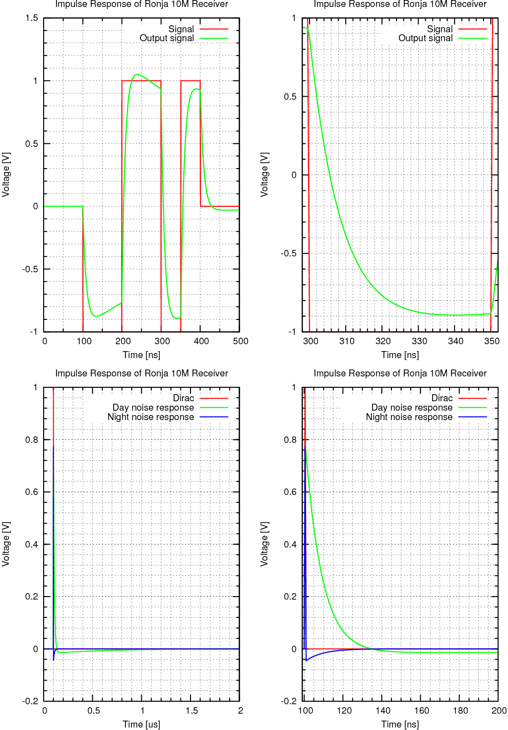
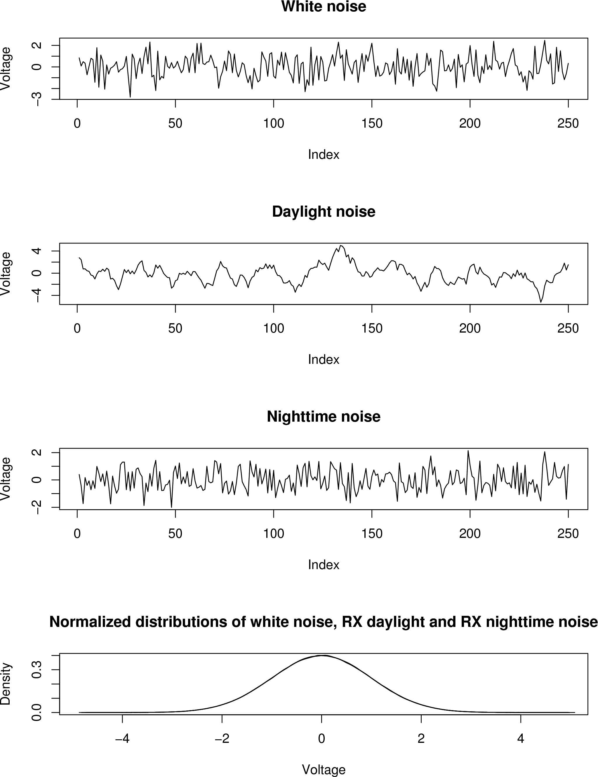
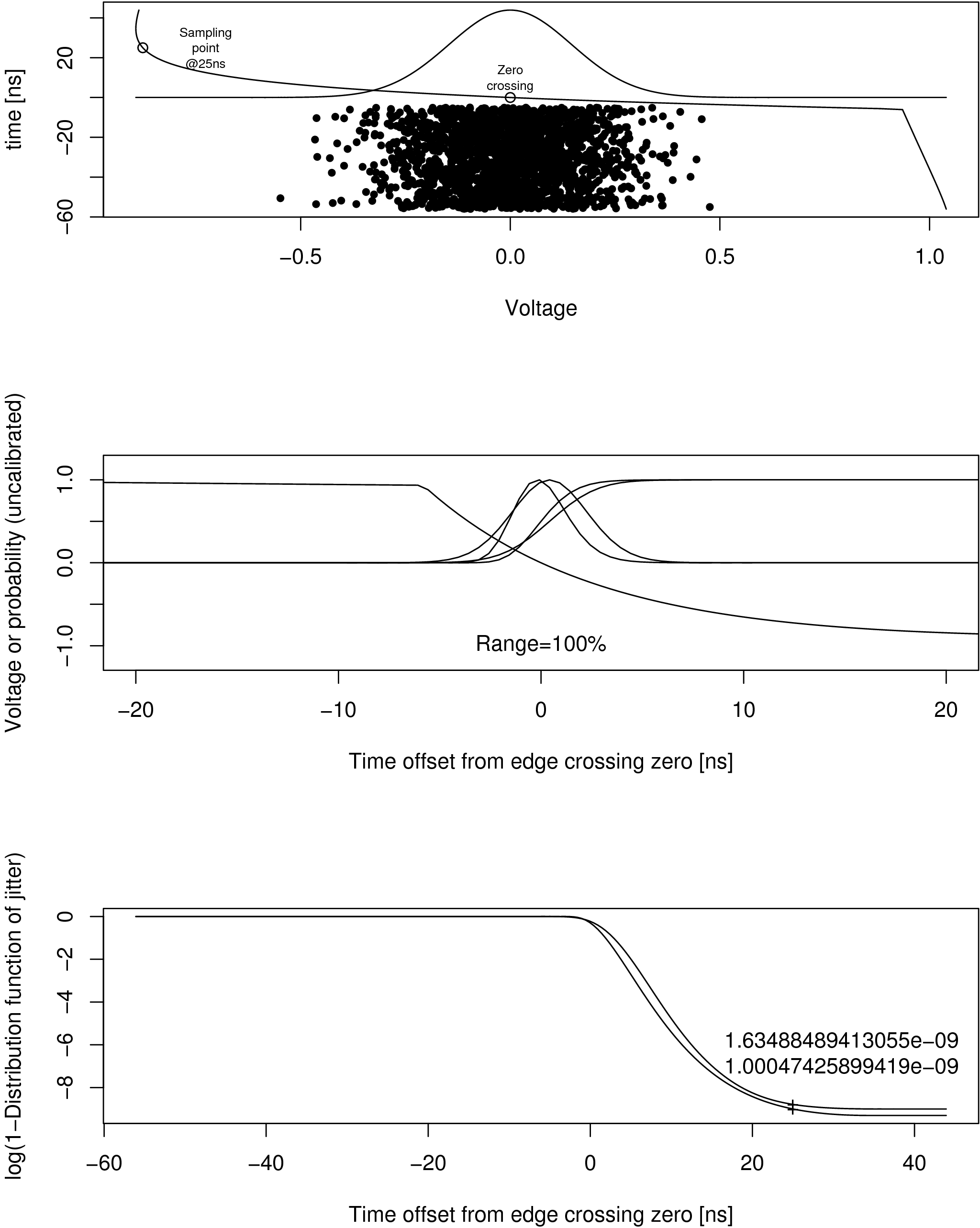
The white noise generated in amplifier prior to having it's spectrum changed is Additive white Gaussian noise (AWGN). Simulation and processing by GNU R reveals that the receiver noise, both daylight and nighttime, have probability distribution that is Gaussian as well.
The same can be inferred theoretically as well. We want to prove that the resulting noise at the output of the receiver will have Gaussian distribution. The impulse response of the receiver can be expressed as a train of samples. AWGN coming into the process has every sample independent and distributed according to Gaussian distribution. When scaled by the individual values, the Gaussian distributions change their standard deviation. Multiplying by -1 doesn't change properties of Gaussian distribution because it's symmetric. When the values scaled by the kernel are summed together, we use theorem about Sum of normally distributed random variables, which tells us that the result will be also Gaussian.
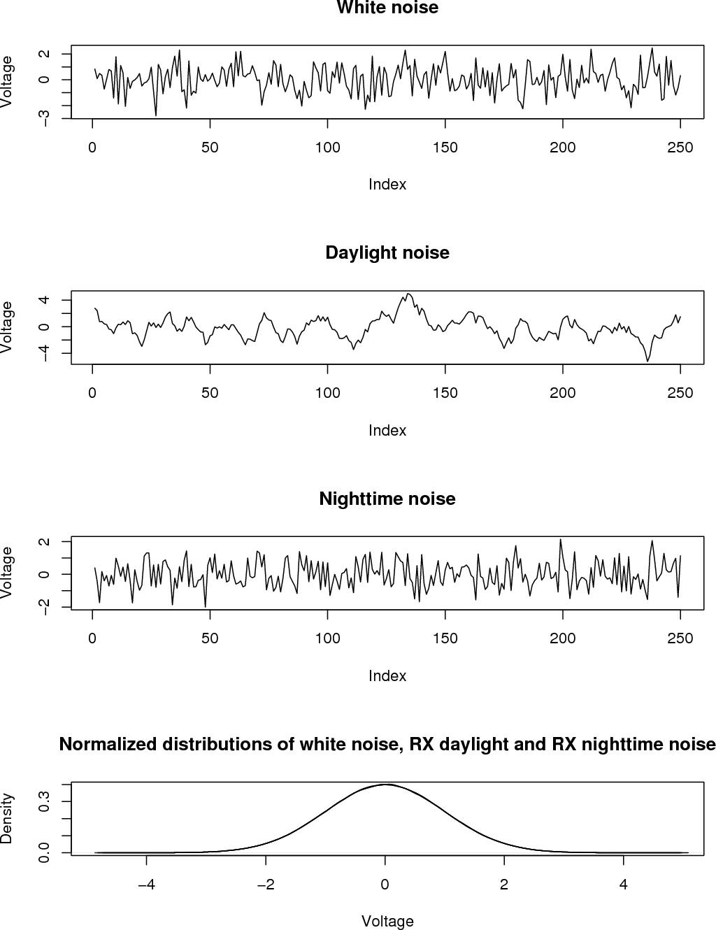
The first graph on left shows signal edge with sampling point. The noise is shifting the edge left and right (on voltage axis). If the signal is shifted by the noise so much that the sampling point gets into positive voltage range, then it's interpreted as different bit value and bit error occurs. The trailing edge was taken from previous picture to the right from around 300ns. The noise indicated is calculated to cause 10^-9 BER.
The second graphs shows the edge and density and distribution functions of time jitter. Time jitter is that the noise is added to the signal which shifts the edge in time (because the edge is not vertical, but has certain slant). After requantizing (forcing the signal into 0 or 1 on limiting amplifier) the edge is then time shifted.
The narrower density function (hill) with the steeper distribution function (slope) indicate noise generated in one track segment. The wider hill and gradual slope belongs to noise generated in two track segments linked together with analogue retranslation.
The third graph shows that the probability of bit error for single track segment is 10^-9 and for two track segments it's higher.
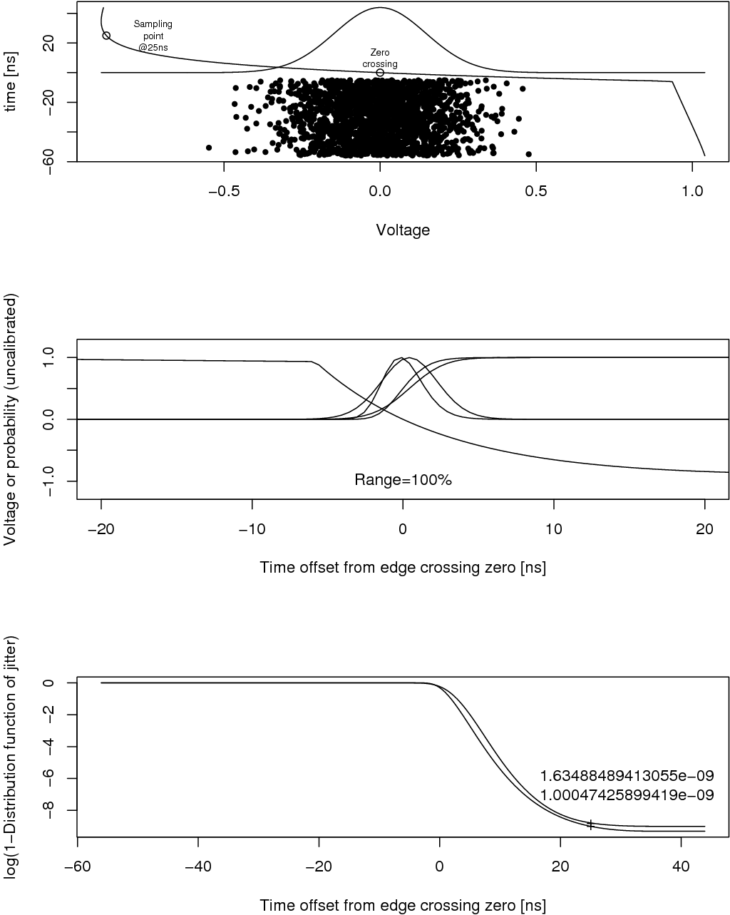
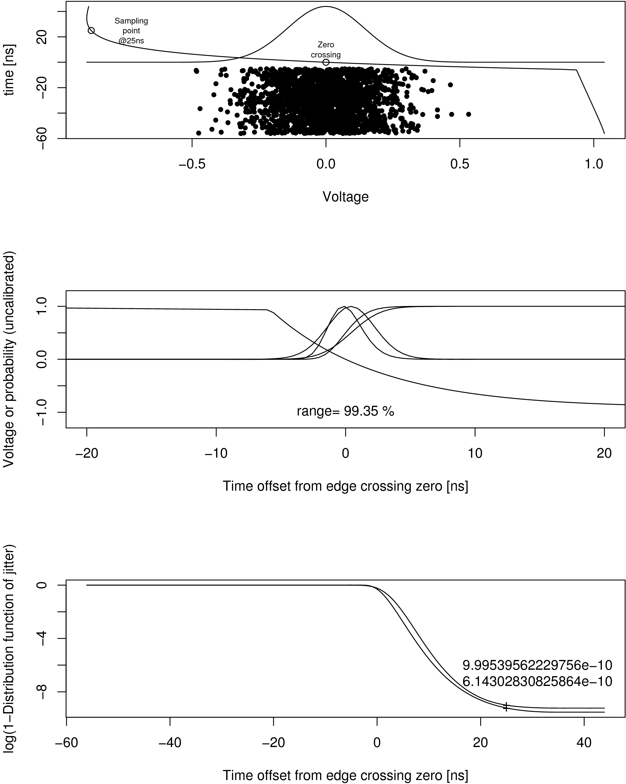
Now we decreased virtually the communication distance which increased the signal and therefore noise is relatively smaller to the signal. We tuned the distance reduction so that after two track segments, the BER is again at 10^-9.
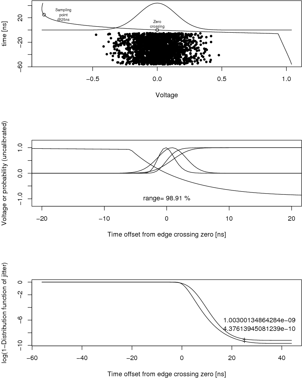
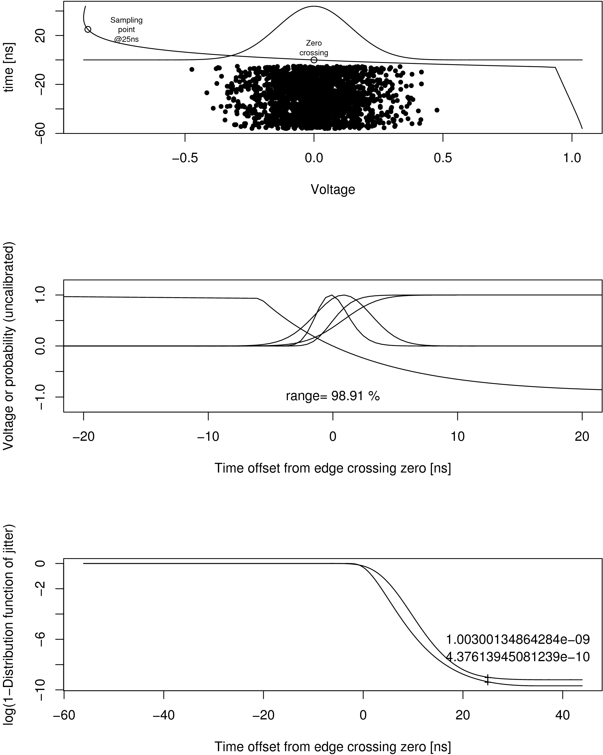
Now we decreased the distance further so the probability of bit error after three track segments is 10^-9. You can see that range reduction caused by jitter buildup on multiple track segments is negligible - for 3 segments the range is reduced to 98.91% (by 1.09%).

 Contact, support: Clock
on the Internet Relay Chat.© 1998-2016 Karel ‘Clock’ Kulhavý et al..
Contact, support: Clock
on the Internet Relay Chat.© 1998-2016 Karel ‘Clock’ Kulhavý et al.. 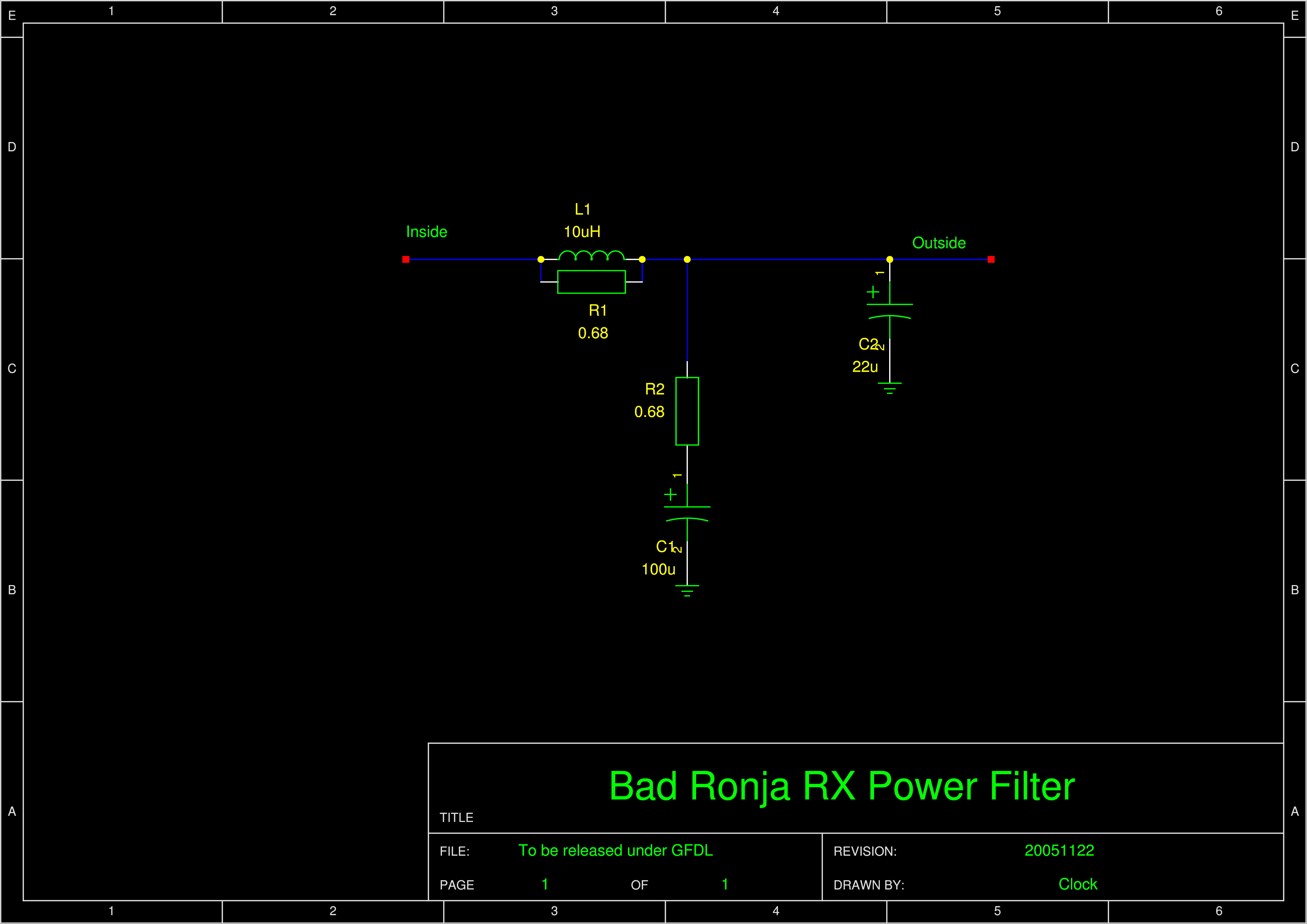


