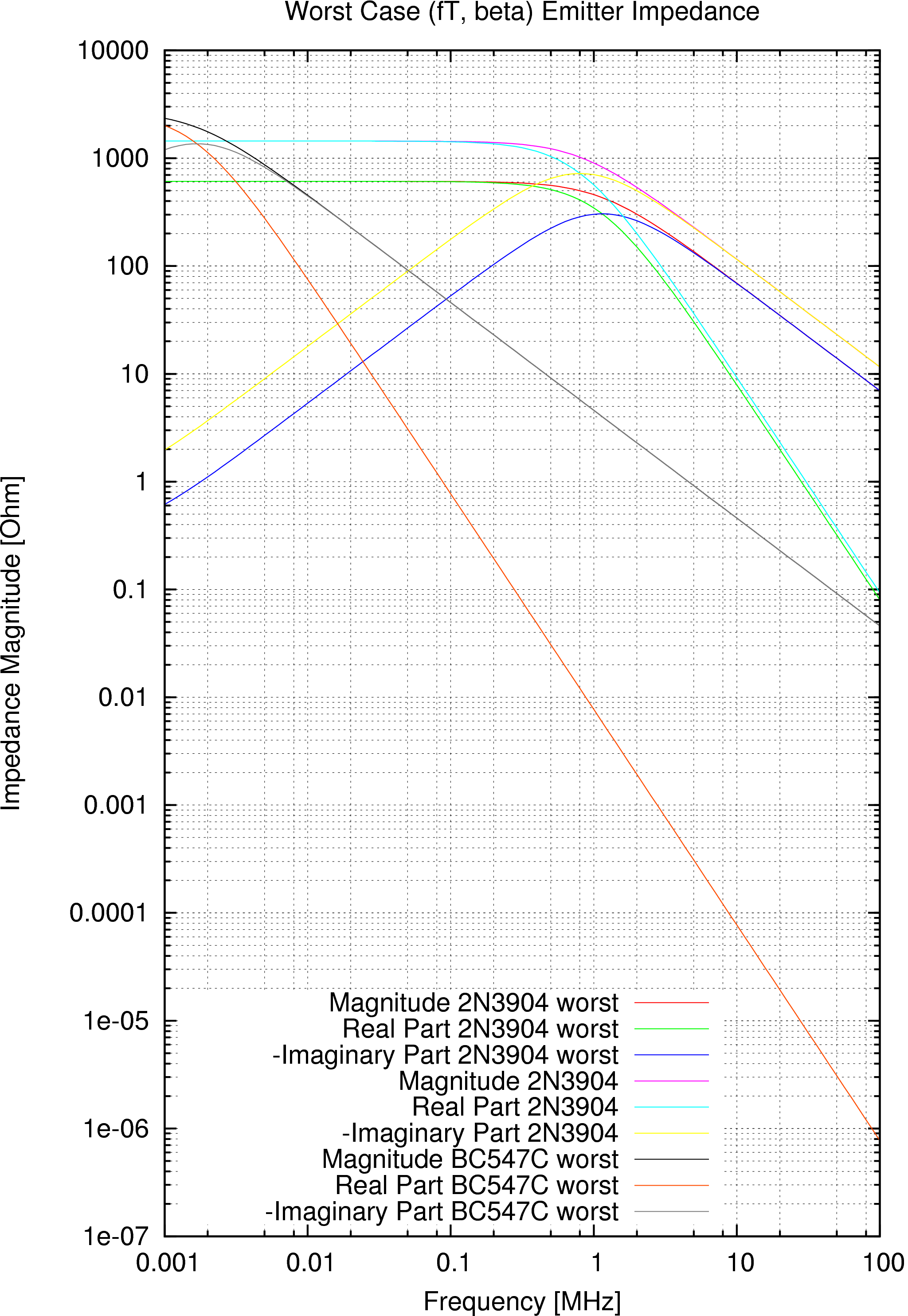
2N3904 and BC547C Emitter Capacitance
|
|
First I wanted to know how big the emitter capacitance of the transistor
under current is.
|
|
|
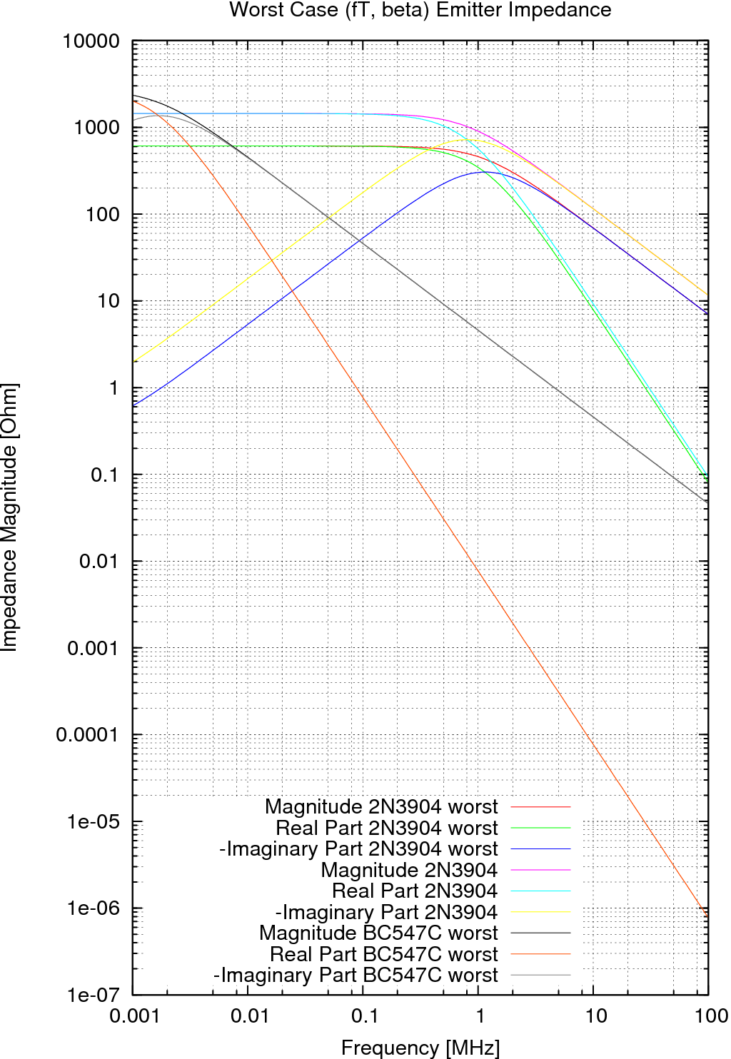
It seems to depend a lot on the transistor type and
less on beta and Ft. BC547C seems to be totally unusable with -48i mOhm
@100MHz which is 33nF!!! Worst case 2N3904
(beta=80, fT=300 MHz) has impedance of -7i Ohm @100 MHz which is 227pF.
Let's assume 3 limiting stage and one MOSFET amplifier, together they have
bandwidth of 16MHz @ -3dB. Each stage should have -0.75dB at 16 MHz. That
means for 227pF we need a 30 Ohm resistor.
|
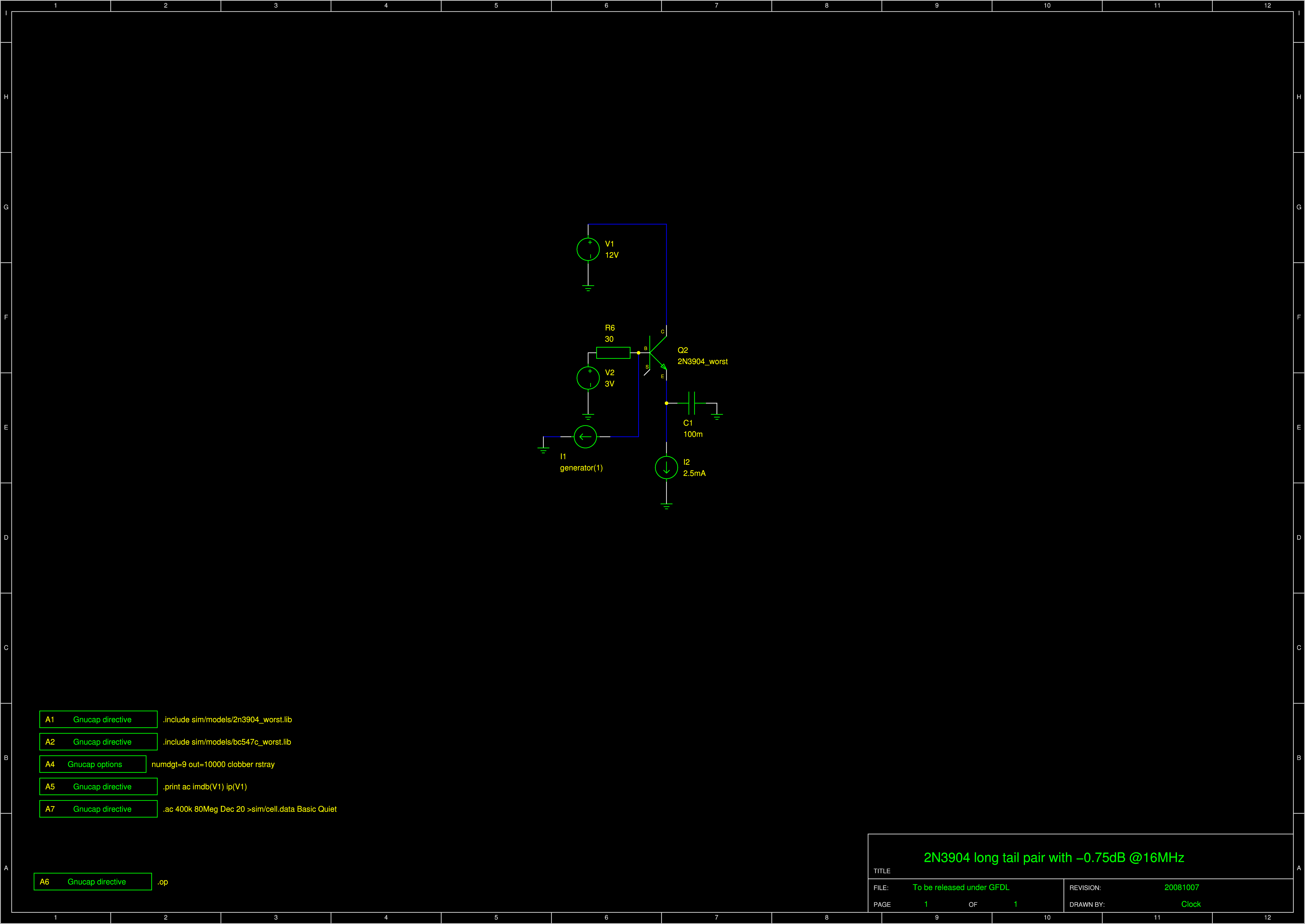
Long Tail Pair With 30 Ohm Resistors
|
|
Let's build a long tail pair with 30 Ohm to counter the 227pF input capacitance.
|
|
|
I had a serious error here. There was accidentally another copy of current
controlled current source (CCCS) which was exactly overlapping the another one and
it was visible only in mangled refdes. This showed -4dB instead of 8dB. The following
headings: Back To The Basics, Sensitivity To Transistor Parameters and Cell Input Impedance
were written with wrong assumption that this stage actually doesn't amplify!
|
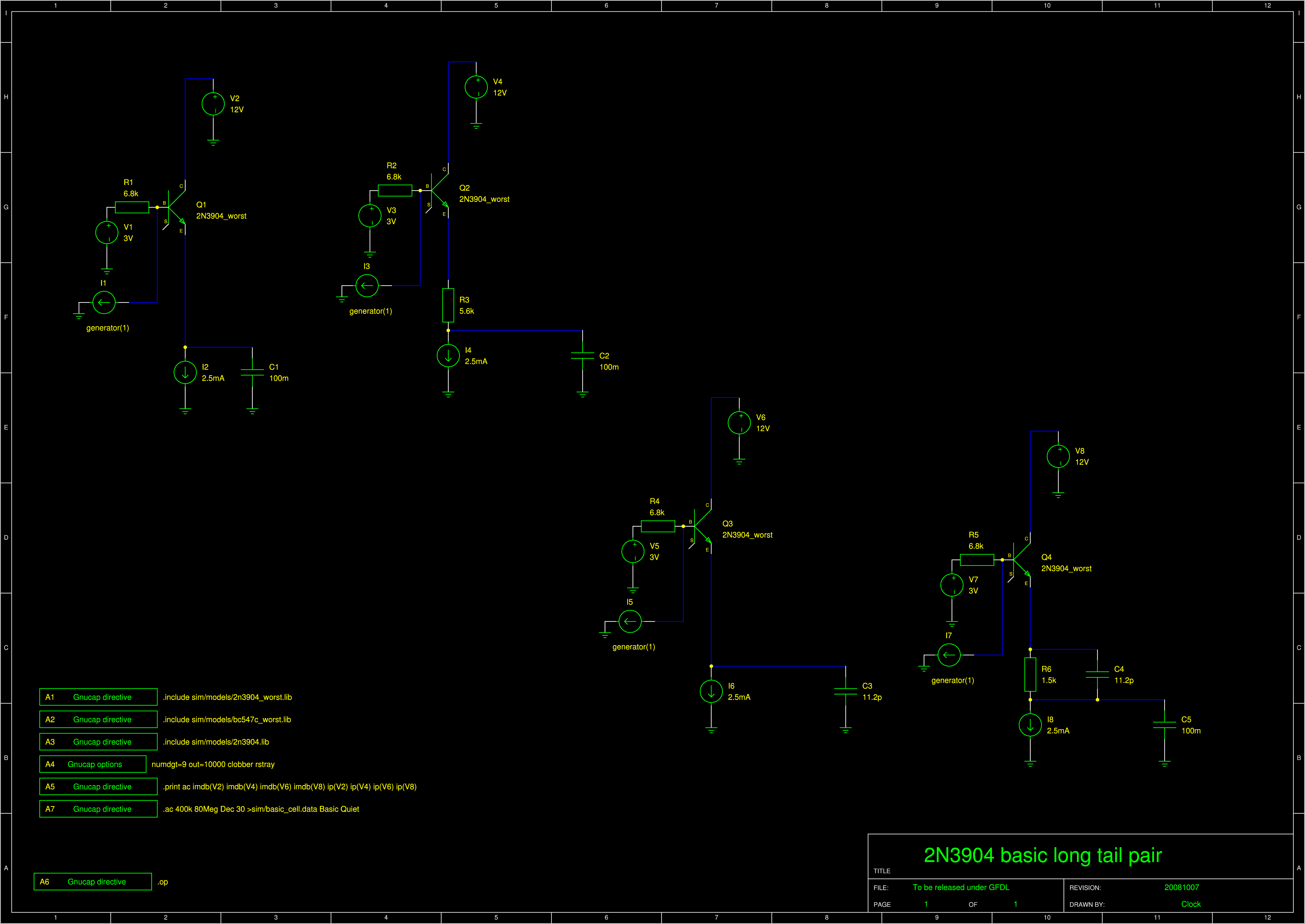
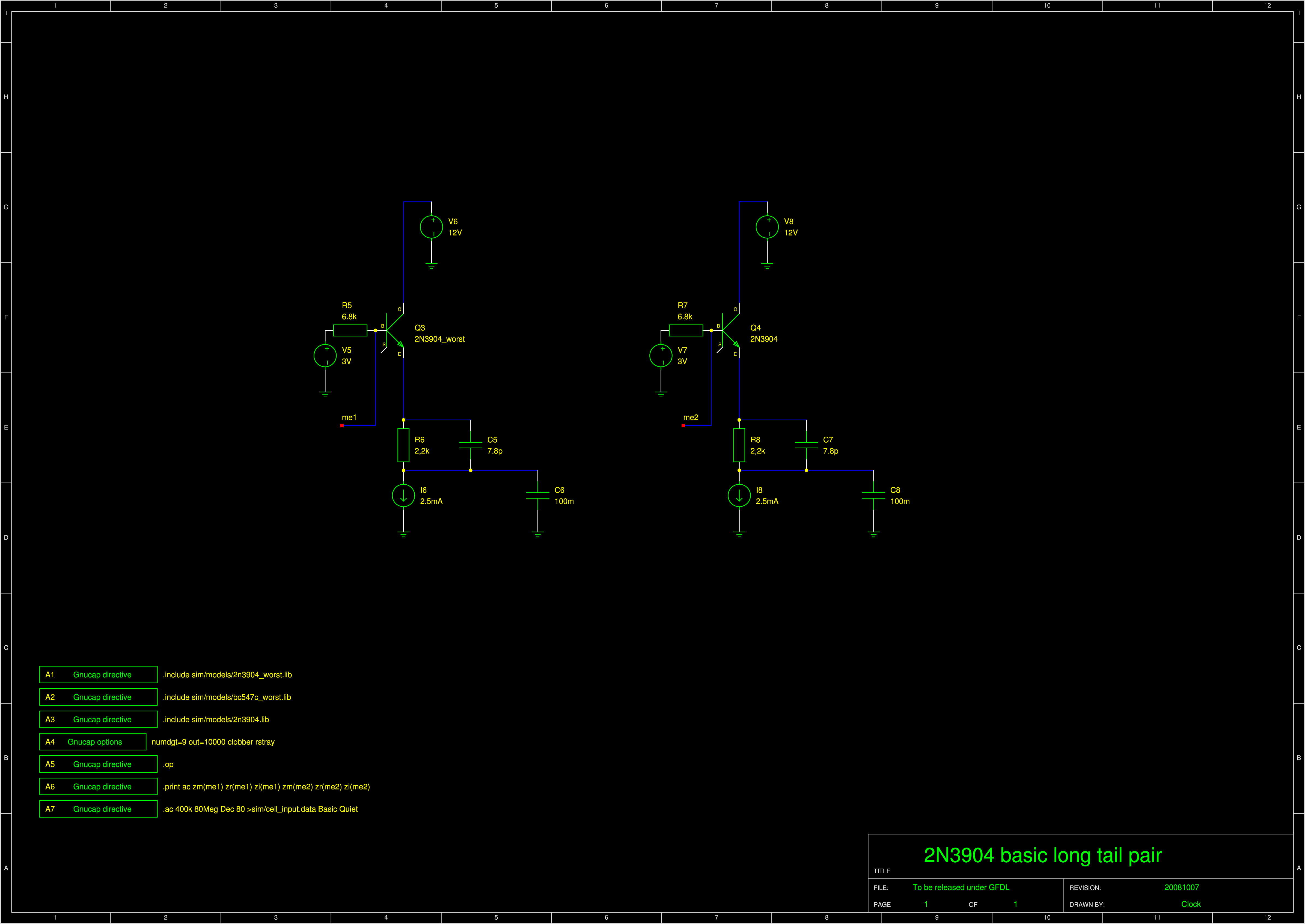
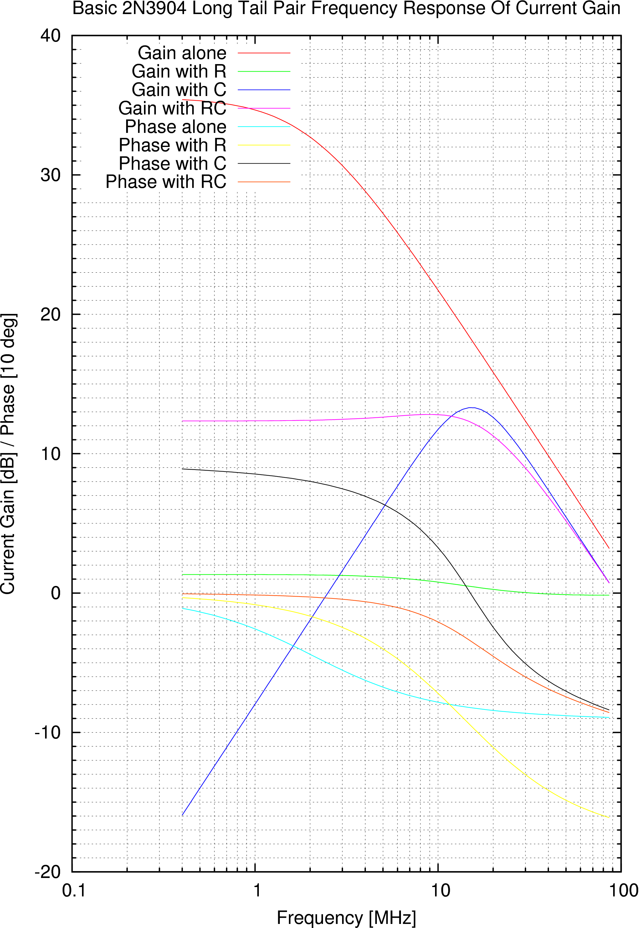
Back To The Basics (written with wrong assumption)
|
|
What's the problem with the basic long tail pair without any resistors?
|
|
|
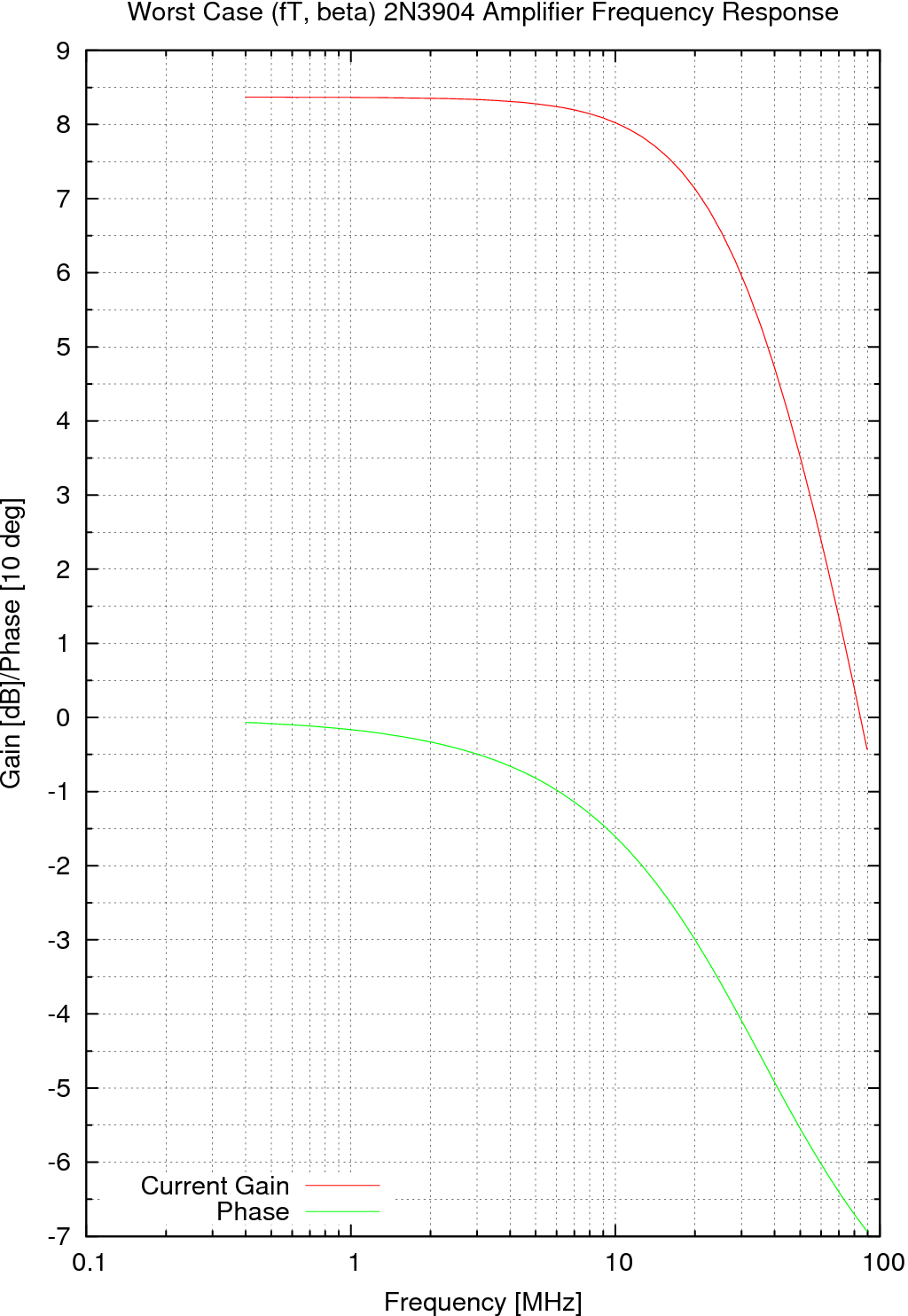
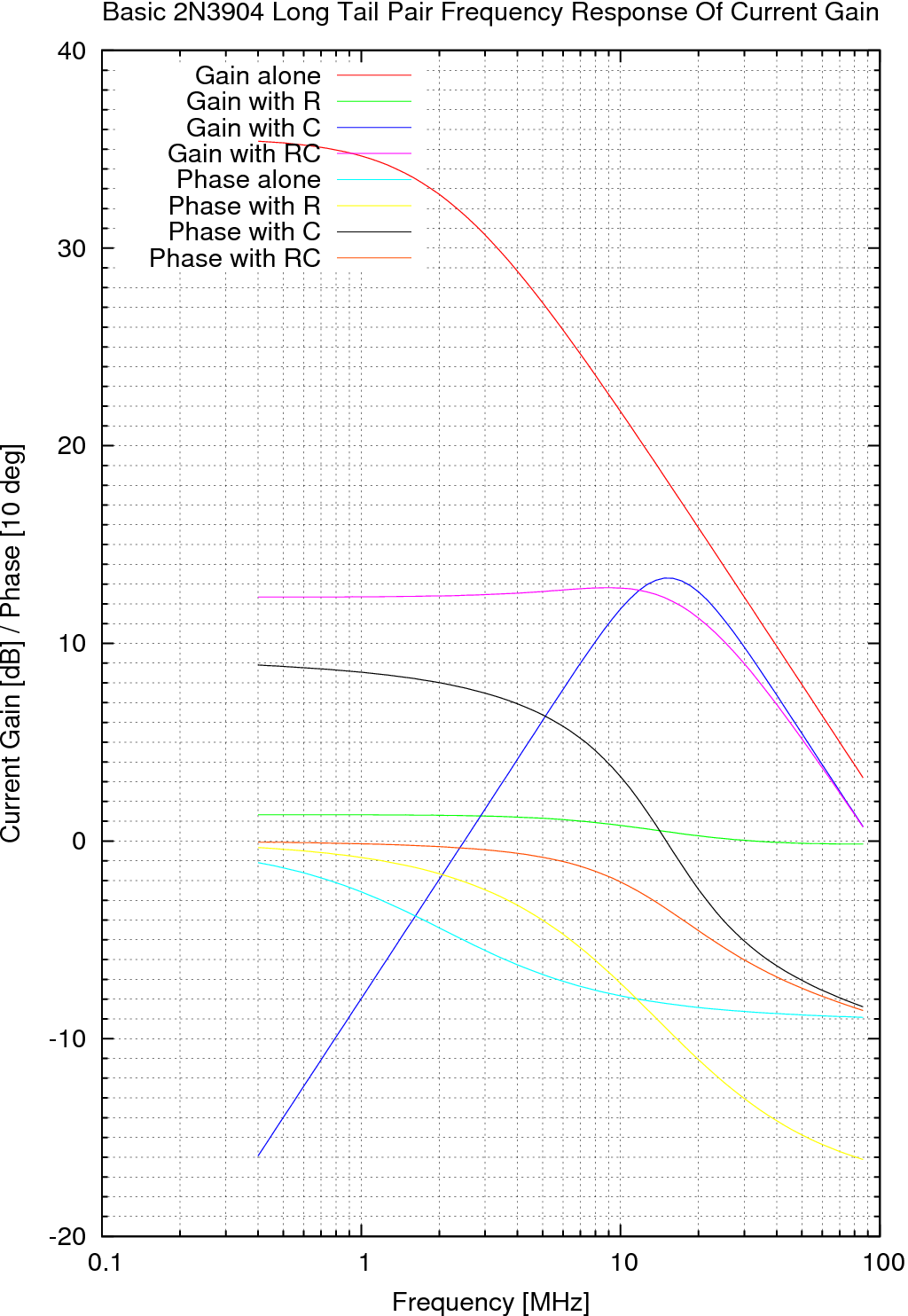
The problem is that the current gain gets bigger for lower frequencies which
distorts the signal significantly, it acts like an integrator. At 16MHz we have 18.5dB of
gain. If we could cleanly cut off the excess gain at lower frequencies,
we would get an amplifier with 19.25dB gain and -0.75dB bandwidth of 16 MHz.
One approach is put a resistor into the emitter. That will limit the
maximum gain. Unfortunately the achieved gain of 1.3dB is laughable.
Another one is put a capacitor into the emitter which acts similar to a resistor
that increases with decreasing frequency. Unfortunately interaction of the capacitor
with the guts of the transistor produces a resonant behaviour. I tried to change
the value and the peak was rising suggesting oscillation is close.
I selected the C to create a peak at the edge frequency of 16MHz.
However combining the C from previous try with a custom resistance in
parallel yields a surprisingly good behaviour, amplification of 12.3dB with a
nicely flat characteristics and gentle phase changes. The question is how
sensitive this spectral response is to transistor parameters like beta, fT and
emitter capacitance. We are maybe playing with fire here, we are probably using
impedance gyration to work for us to speed up an otherwise lazy transistor. We
are maybe asking for oscillations.
This is similar to designing a speaker with a bassreflex.
|
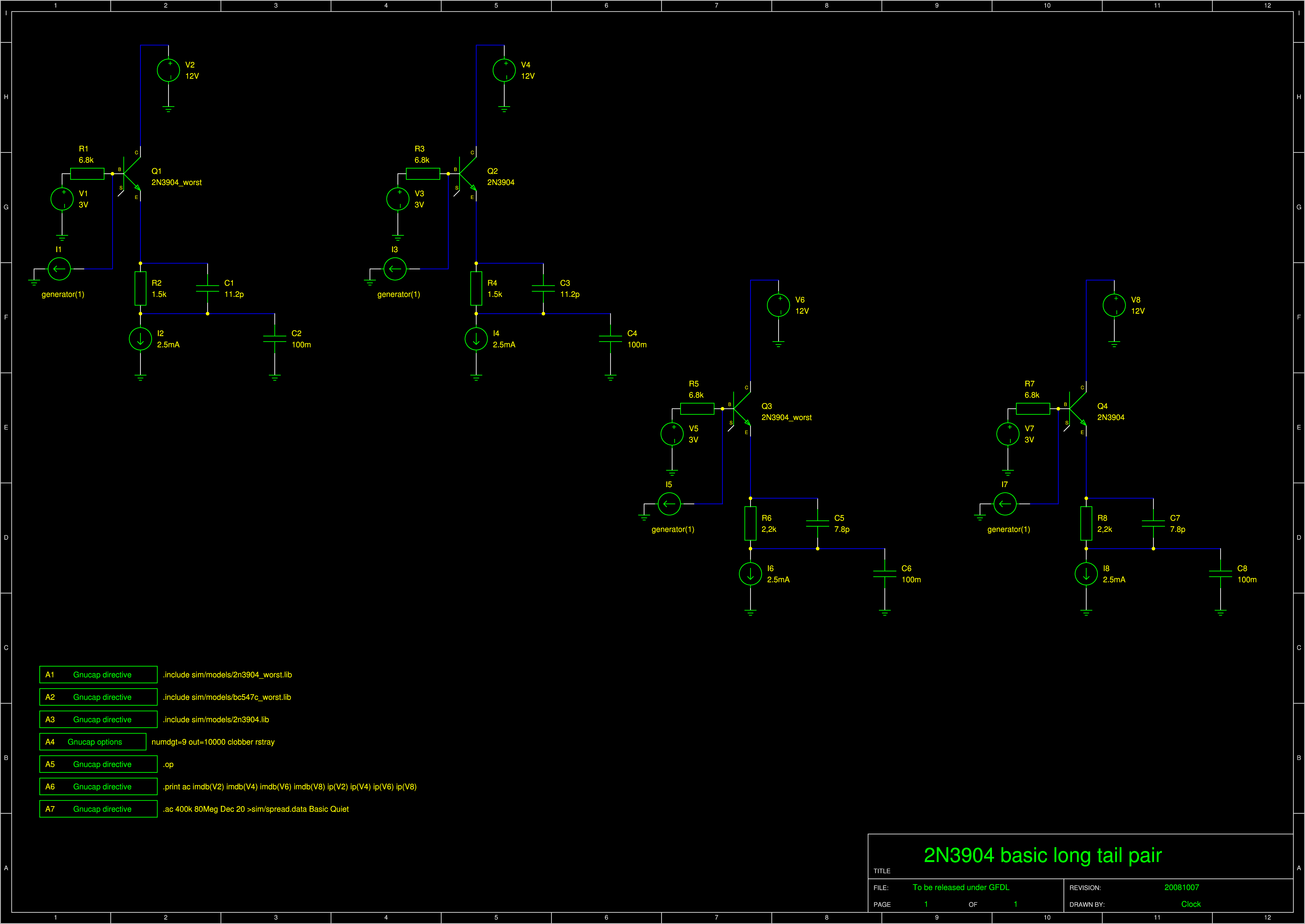
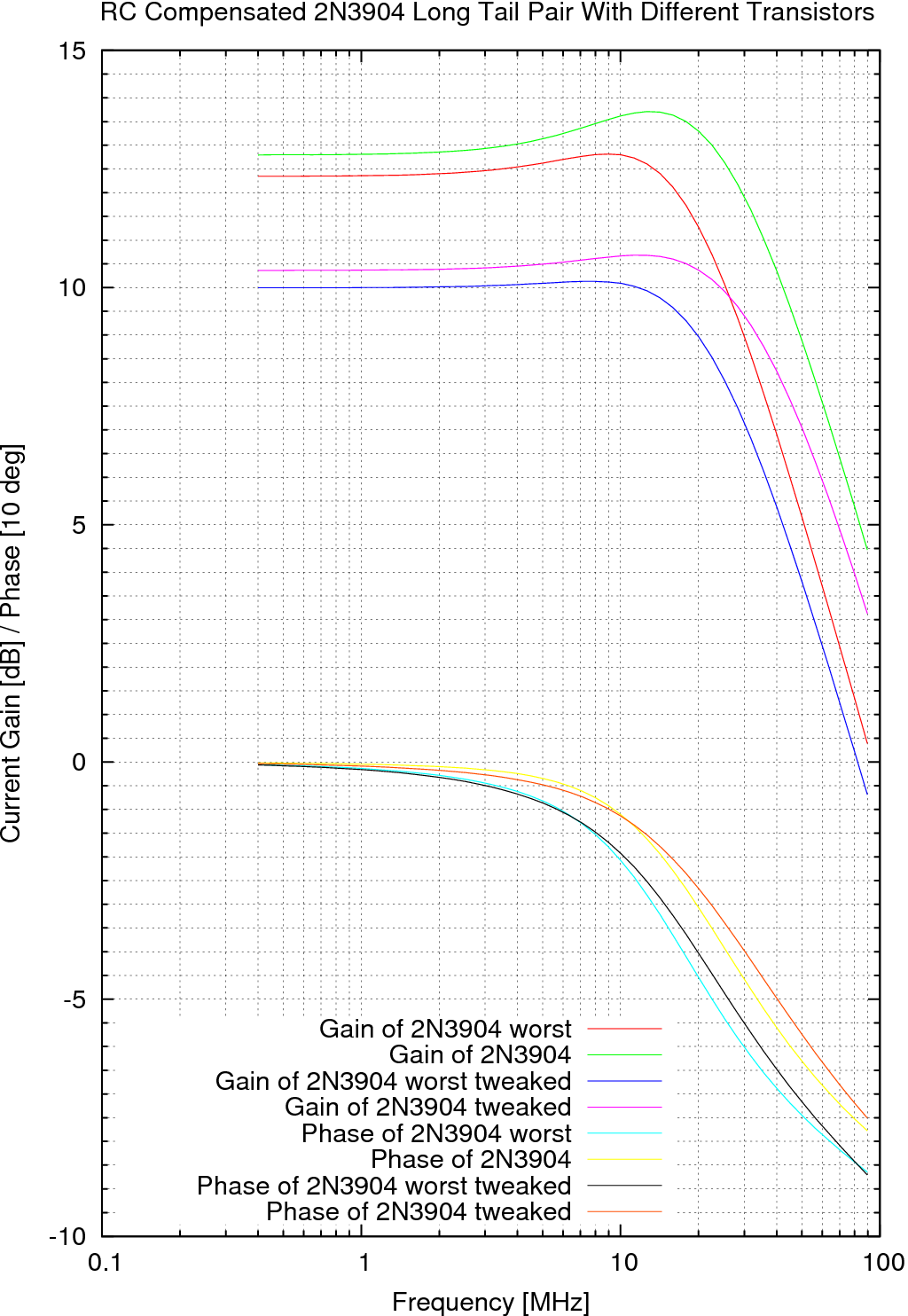
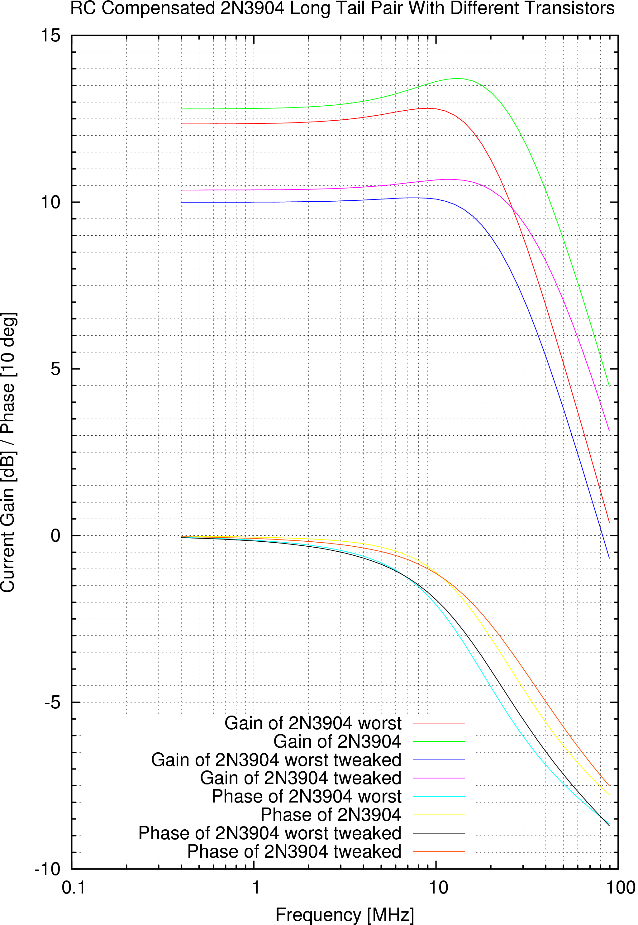
Sensitivity To Transistor Parameters (written with wrong assumption)
|
|
Is the frequency curve going to be sensitive to varying transistor parameters?
|
|
|
Whereas the worst case 2N3904 has 3/4 dB overshoot, the best case has 2dB overshoot.
Let's try to tweak the capacitor and resistor parameters so the charactersitic gets
closer to ideal.
By decreasing the capacitance and adjustingthe resistor the overshoot of the
frequency curve gets to 0.75dB in the worse case and the minimum gain goes
down to 10 dB.
|
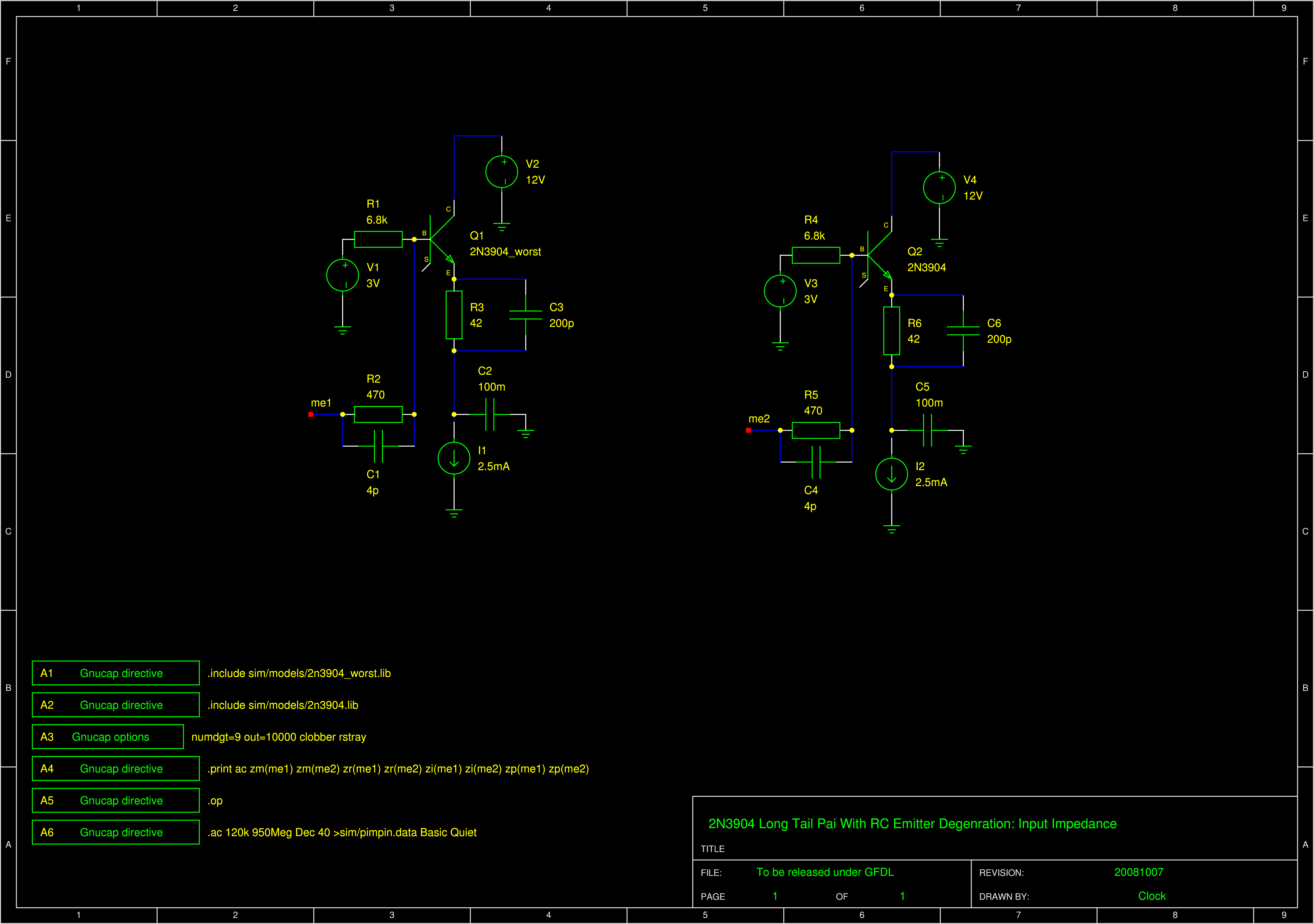
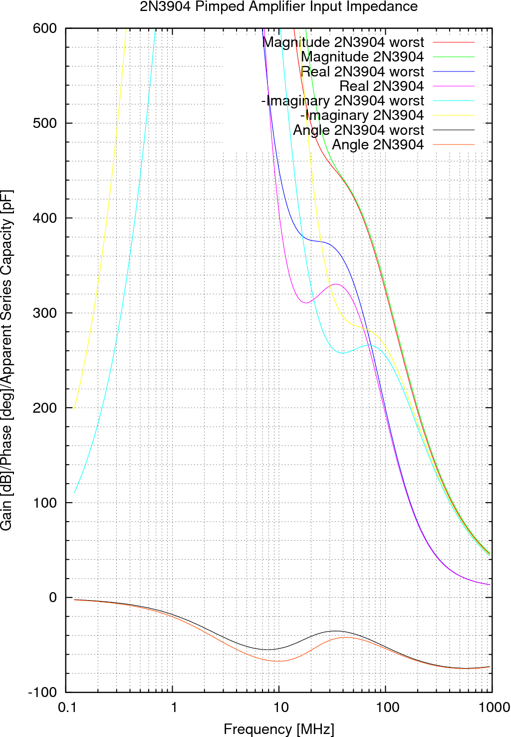
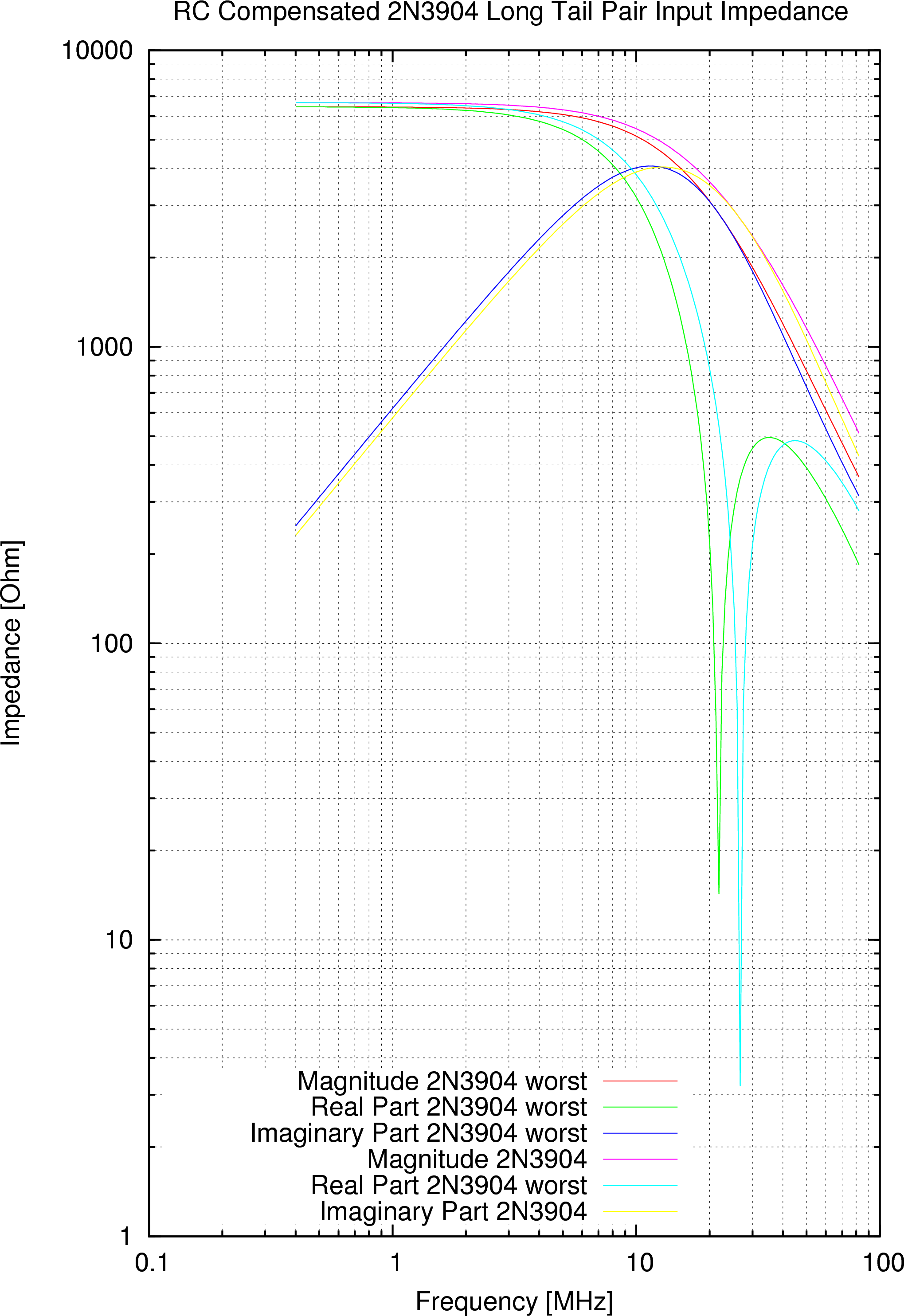
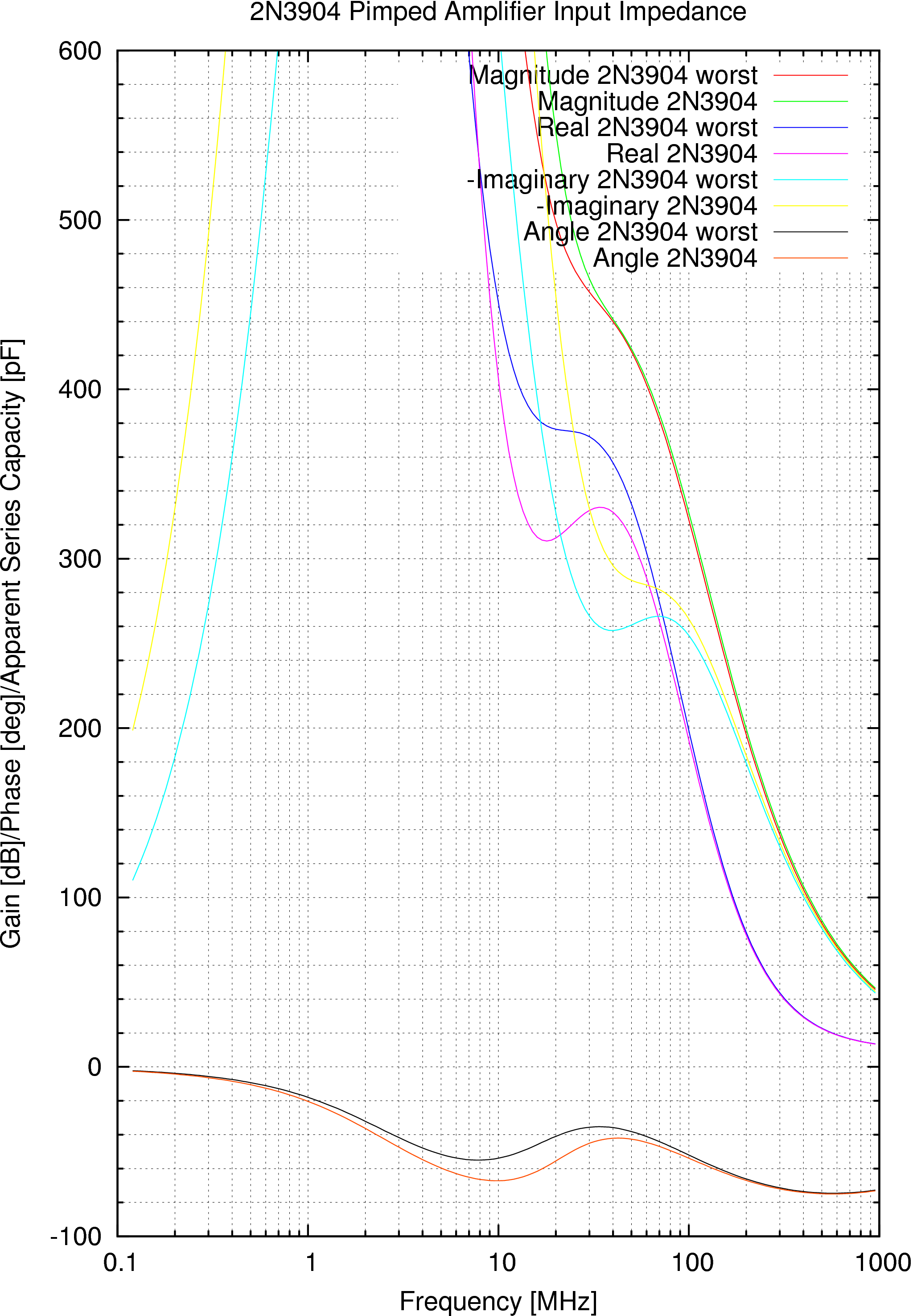
Cell Input Impedance (written with wrong assumption)
|
|
How is the input impedance of the cell going to look like?
|
|
|
Unfortunately the input impedance at 1MHz is 6.5kO. To get the current signal
from the previous stage semi-efficiently into the next one (with a loss of -6dB),
we would need a 6.5kO collector resistor. 6.5kOhm*5mA=32.5Volt. That's way too much
voltage swing.
|
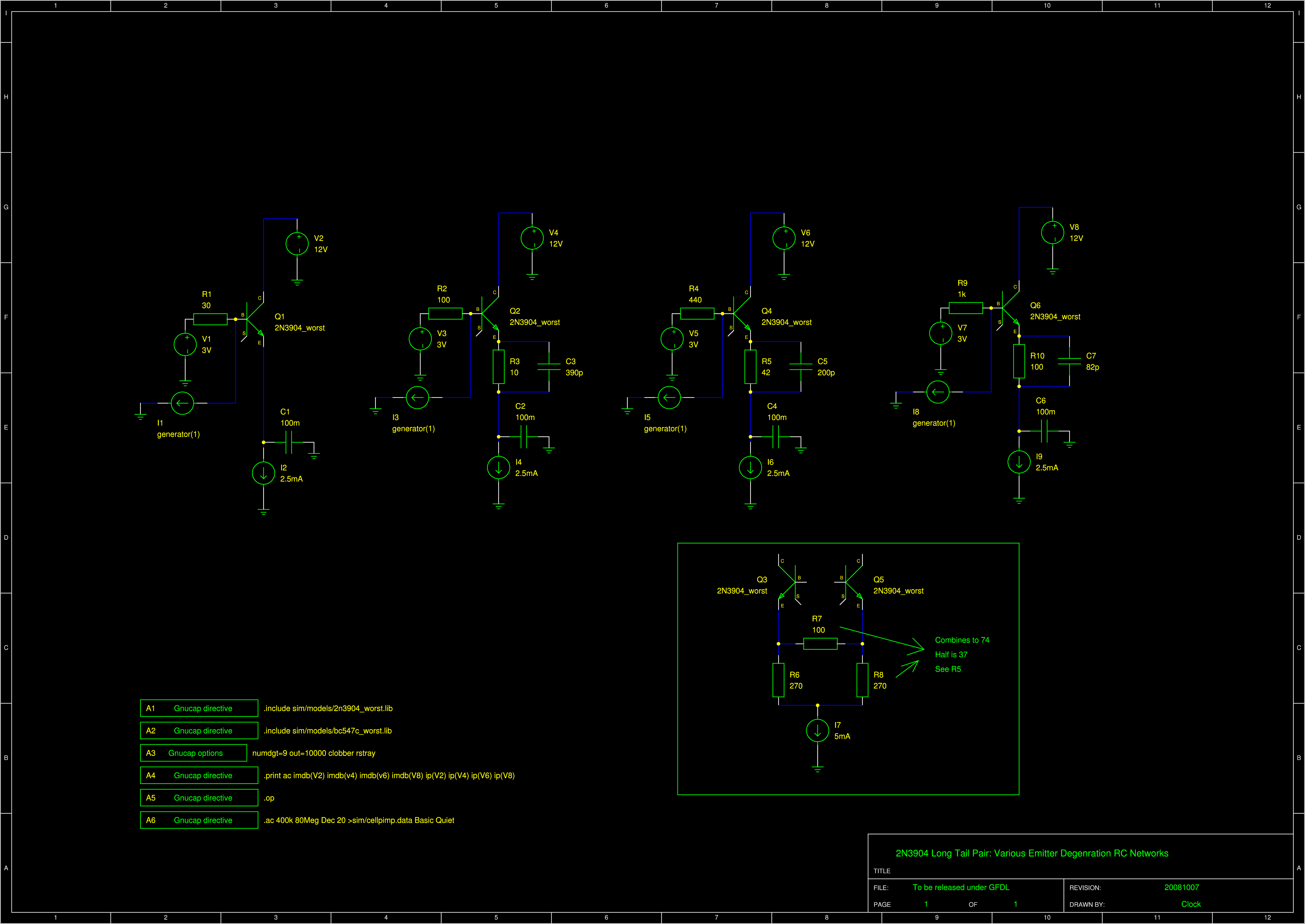
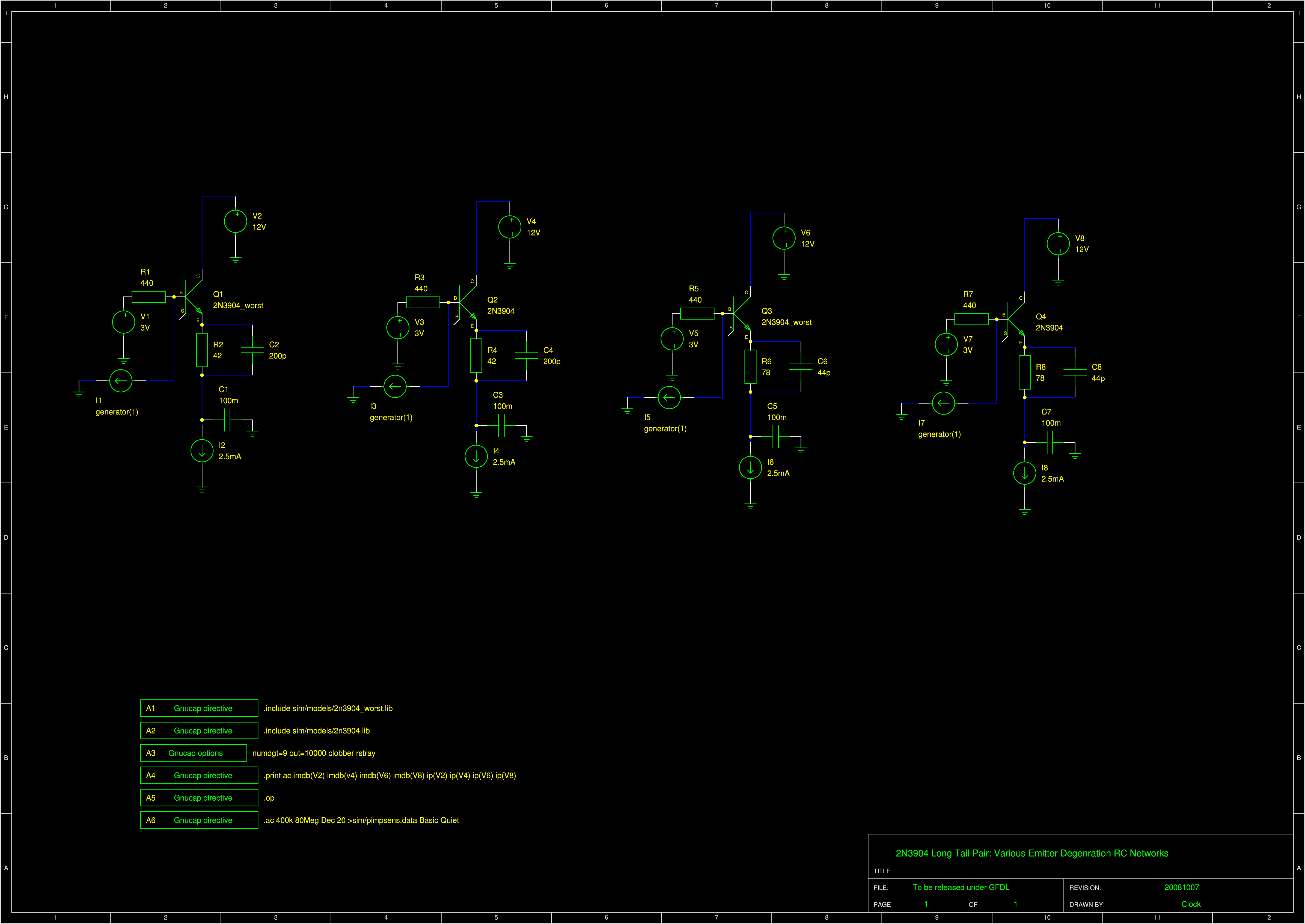
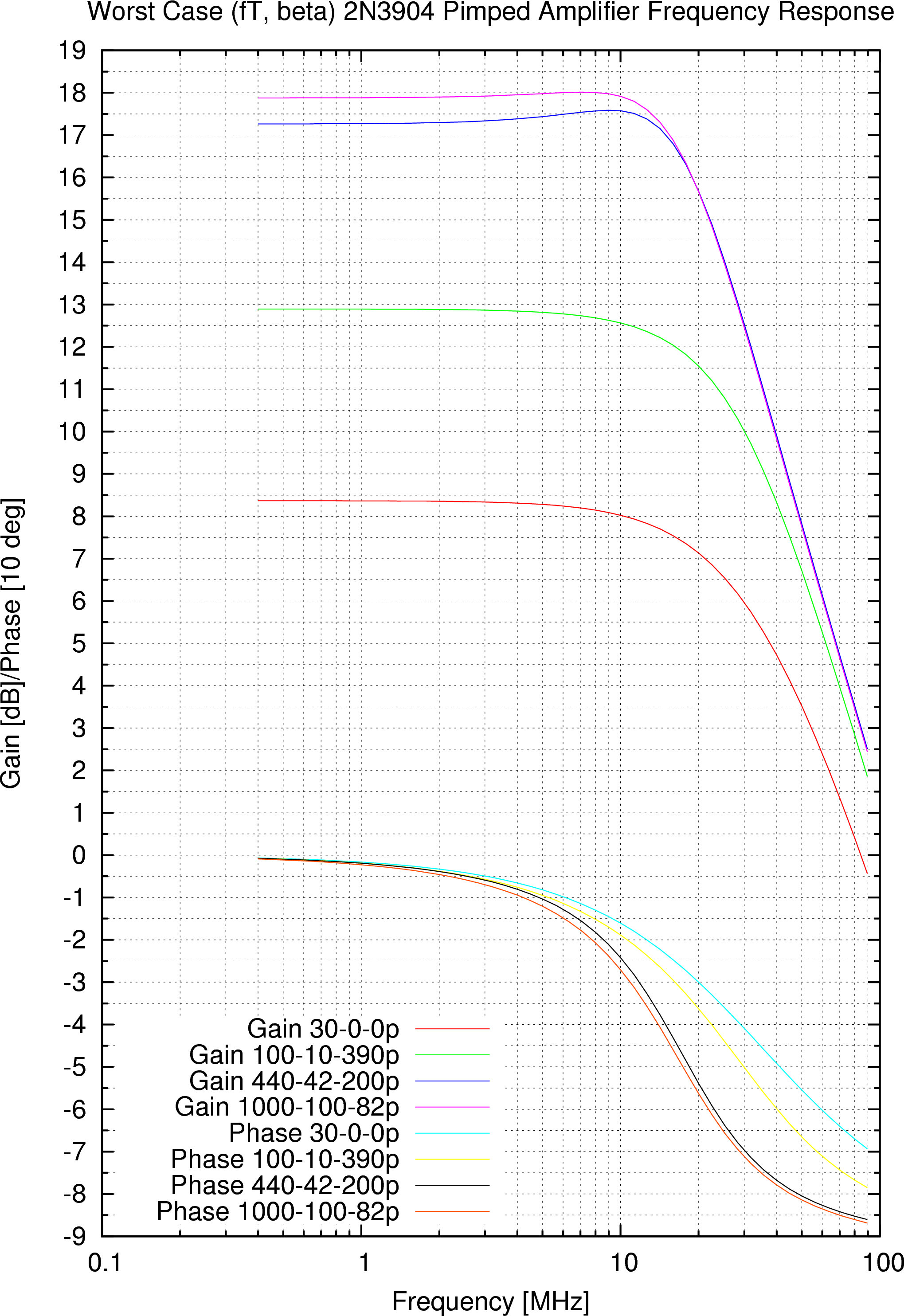
Pimping up the voltage mode cell
|
|
Since I unnecessarily developed here a way how to pimp up the current amplifier
why not try this method on the voltage mode amplifier?
The weird value of 42 Ohm was selected because of transistor mismatch. The
DC gain of 2N3904 varies from 80 to 300 @2.5mA. That's a ratio of 1:3.75.
Natural logarithm 1.32. With 26mV per e-times it makes 34mV difference in base
voltages. If we want imbalance 1:20 then the drop on the balancing resistors must be
690mV. With 2.5mA current per balancing resistor it makes 270 Ohm. With a 100 Ohm
resistor it makes the desired response. The resulting total resistance for
the simulation is then 42 Ohm.
I want to limit the differential signal to 2.2mVpp to not lose too much
headroom for the transistors. That means collector
resistors of 470 Ohm. With my usual 6.8k base resistor in paralle it makes 440
Ohm. That's the other weird value in the simulation.
|
|
|
The pimp up method seems to be very powerful. We can increase the gain from 8.4dB to
18.3dB. Here is a table of component values and achieved gains:
| Base resistor | Emitter resistor | Emitter capacitor | Gain |
| 30 Ohm | 0 Ohm | 0pF | 8.4dB |
| 100 Ohm | 10 Ohm | 390pF | 12.9dB |
| 220 Ohm | 18 Ohm | 390pF | 16.6dB |
| 440 Ohm | 42 Ohm | 200pF | 17.4dB |
| 470 Ohm | 39 Ohm | 220pF | 18.3dB |
| 560 Ohm | 56 Ohm | 120pF | 17.4dB |
| 1000 Ohm | 100 Ohm | 82pF | 17.9dB |
|
Pimped Up Cell Stability
|
|
According to Why Circuits Oscillate Spuriously by Dennis L Feucht,
Putting a RC network into the emitter of a common collector amplifier (which we still have,
since the collector is nailed down to the voltage source) is a way how to possibly make
it oscillate. I have to check if the input impedance has a negative resistance somewhere.
|
|
|
The simulation show what impedance a coil between the previous stage and our base
sees. There is no negative resistance. The coil will not oscillate no matter
how big it is.
|
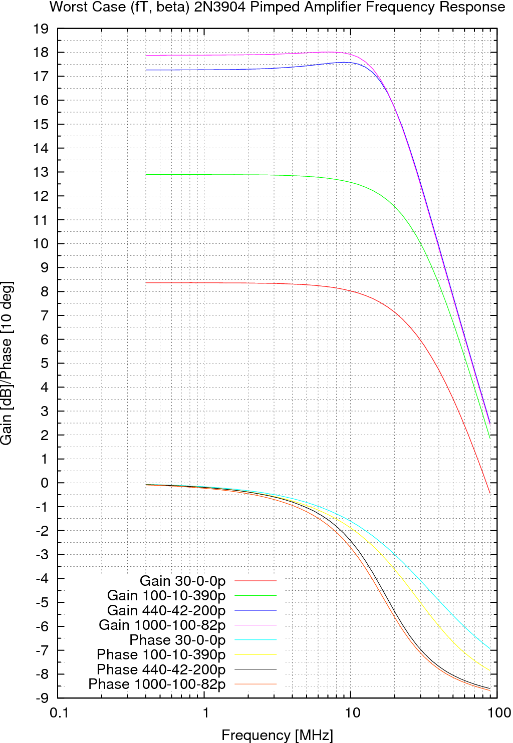
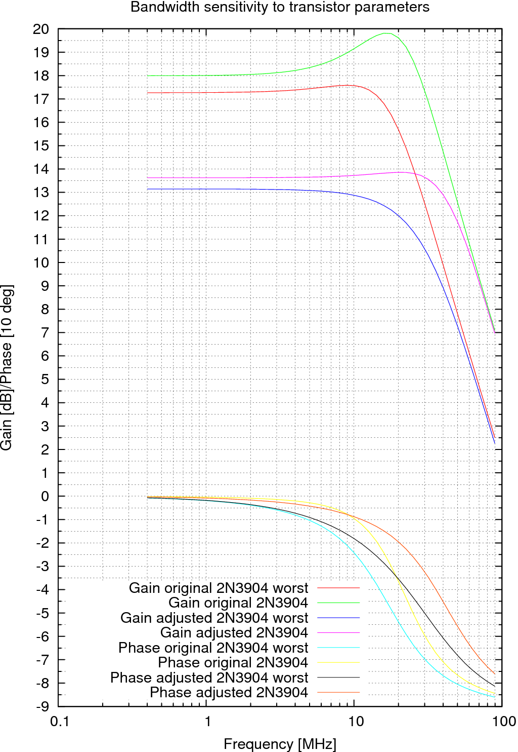
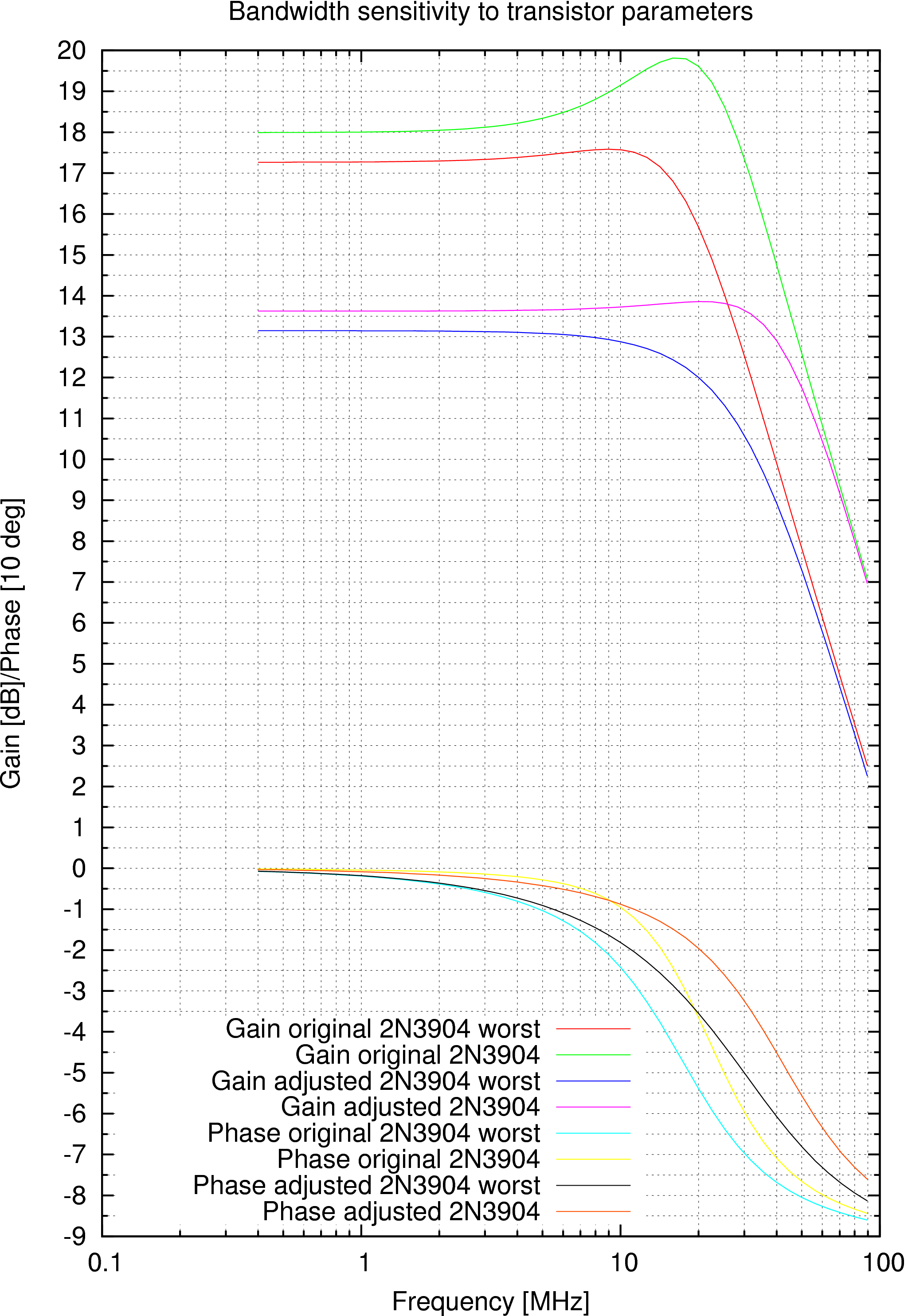
Pimped Up Cell Bandwidth Sensitivity To Transistor Parameters
|
|
What happens with the frequency and phase response when we replace the worst case
2N3904 with a normal 2N3904?
|
|
|
We see a 2dB hump occurs on the end of the response. With 3 stages this will create
a 6dB hump which is probably not tolerable. Therefore I adjusted the emitter degeneration
to not be so agressive. However it's a tradeoff against gain of course.
|
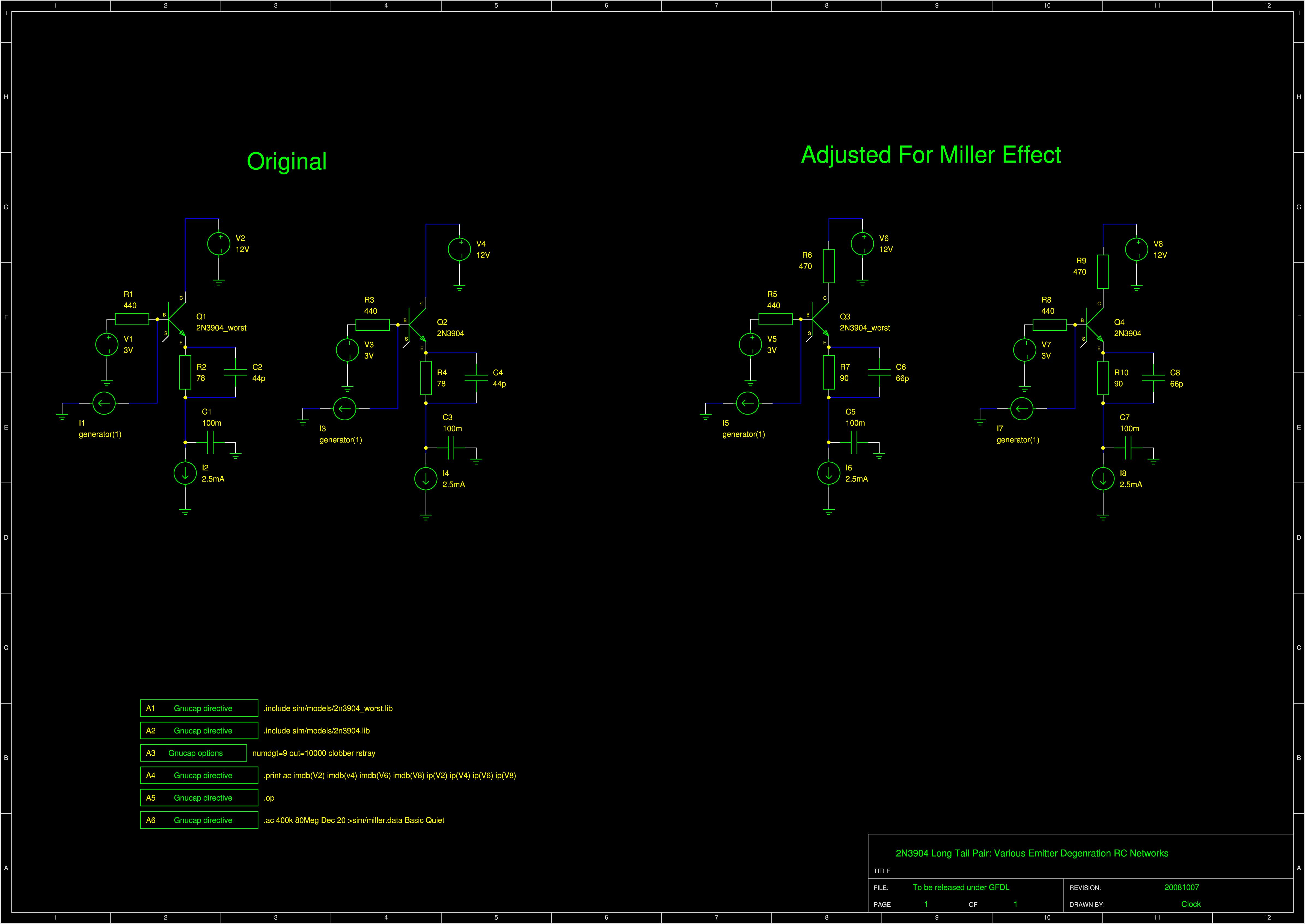
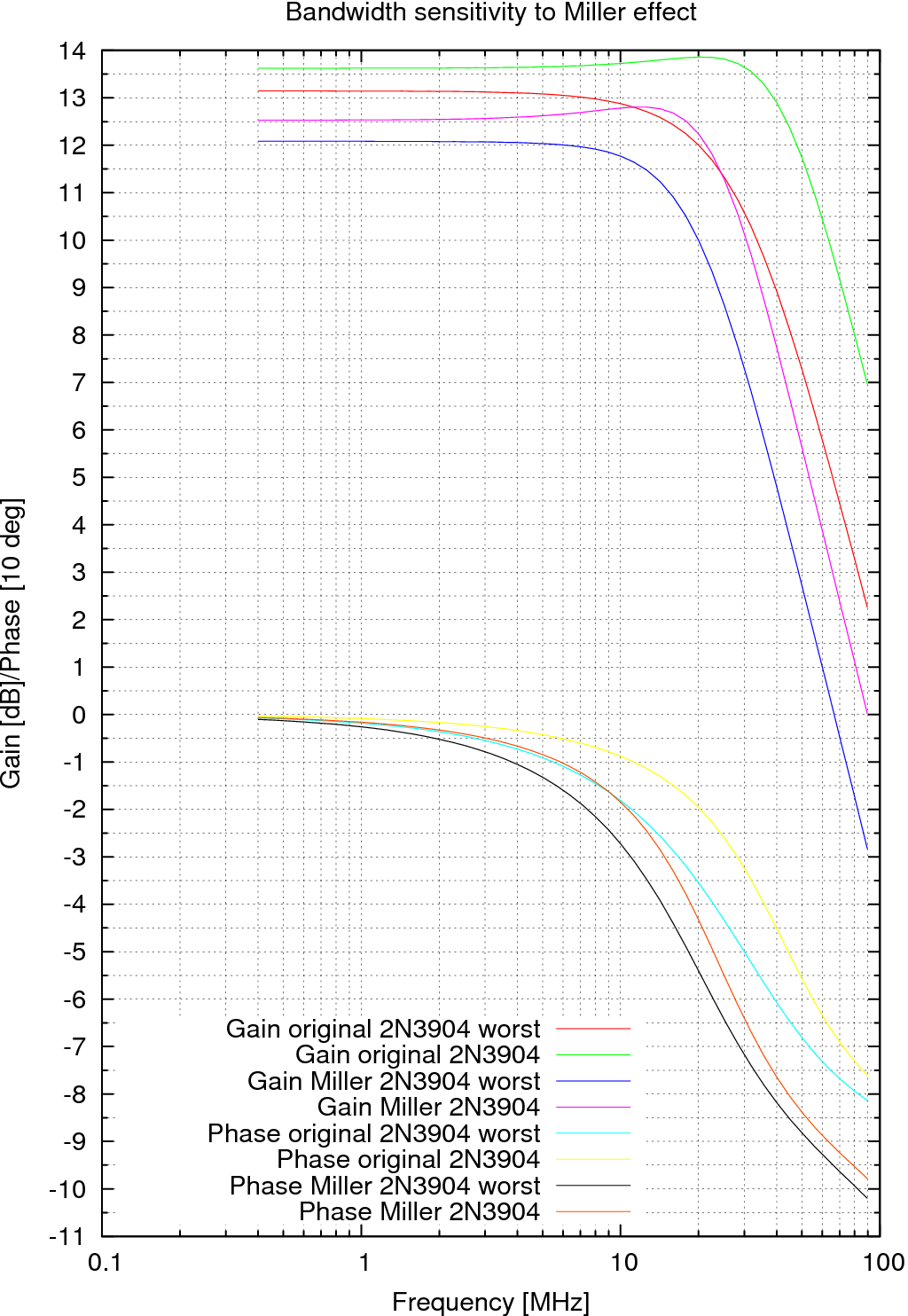
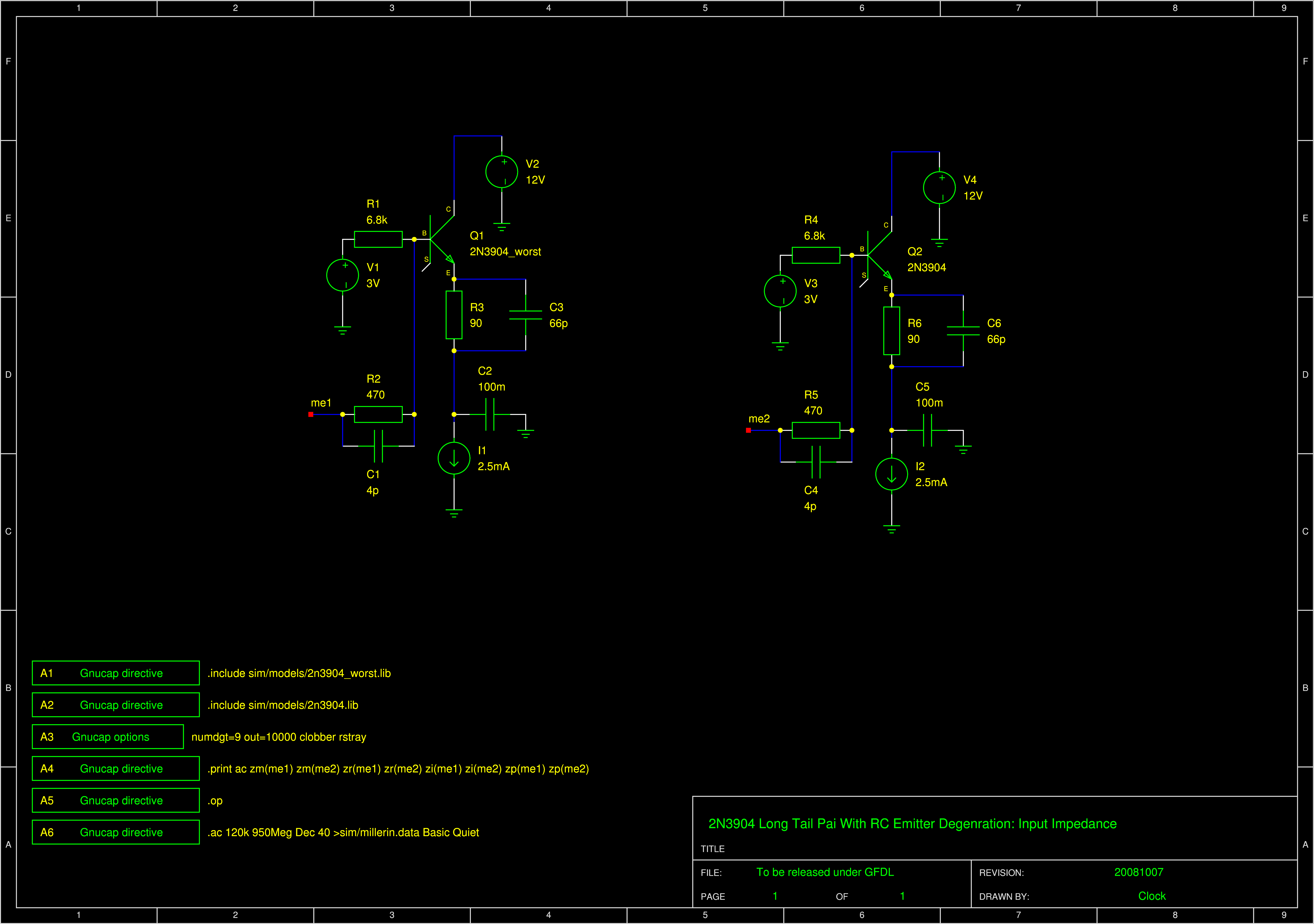
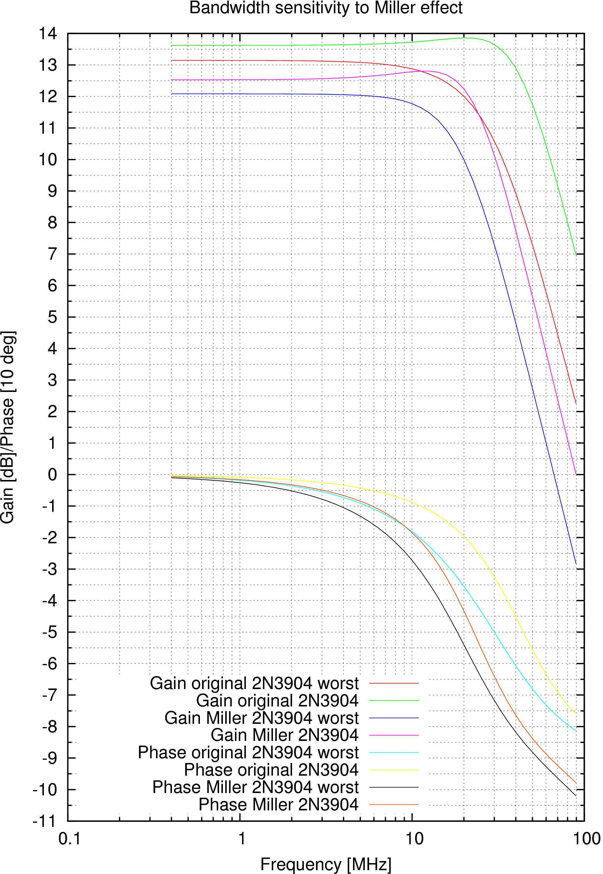
Bandwidth Sensitivity To Miller Effect
|
|
What happens with the frequency and phase response when we stop holding the
collector at a constant potential and insert the working resistor? Miller
effect will kick in.
|
|
|
After turning the Miller effect on the bandwidth dropped to about 7MHz. So I
tuned the emitter degeneration again. The minimum gain dropped from 13.2
to 11.7dB. This doesn't justify cascode because cascode has 5 transistors and
without cascode there are only 3 transistors. Therefore the gain would have
to drop under 13.2dB*3/5=8dB.
How is it with phase shift? Phase shift can move 5MHz against 10MHz,
introducing deterministic jitter. If it shifts twice as many degrees @10MHz
as @5MHz, then the waveforms are delayed, but not shifted against each other.
The shifts are as follows:
| Frequency | degrees 2N3904 worst | degrees 2N3904 |
| 5MHz | 12 | 7 |
| 10MHz | 25 | 16 |
For 7 and 16 it's not exactly balanced. The 10MHz is shifted 2 degrees (2 10MHz
degrees) against 5MHz. Since we'll have about 3 stages this is 6 degress @10MHz
or 1.6ns. That's a good deterministic jitter I think.
The 0.5dB hump on Miller 2N3904 will result in a 1.5dB hump after 3 stages. I
guss that's acceptable when the drop at 16MHz will be 3dB.
|
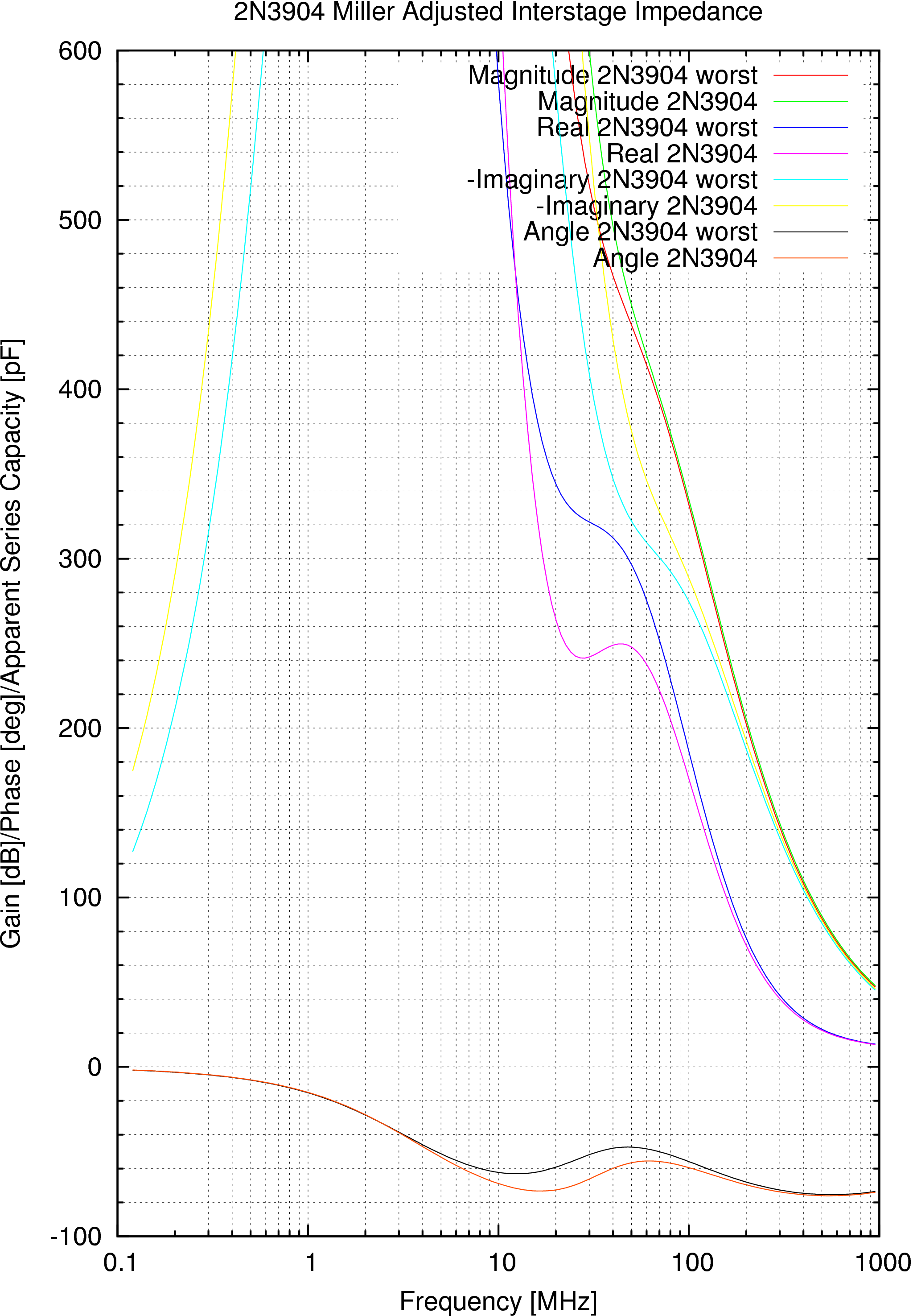
Miller Adjusted Cell Stability
|
|
We have changed the magical element value in the emitter, we have to check for stability
again.
|
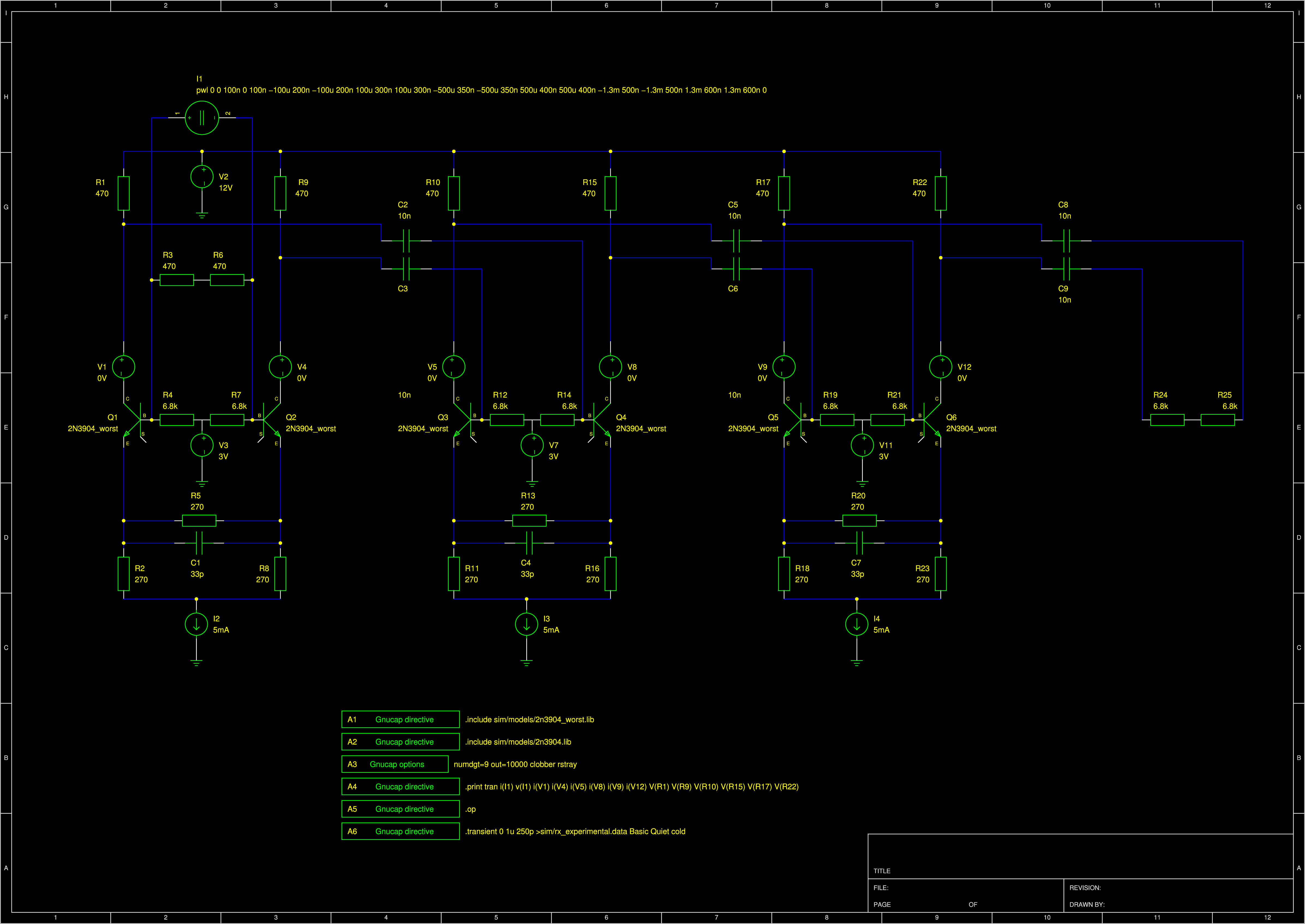
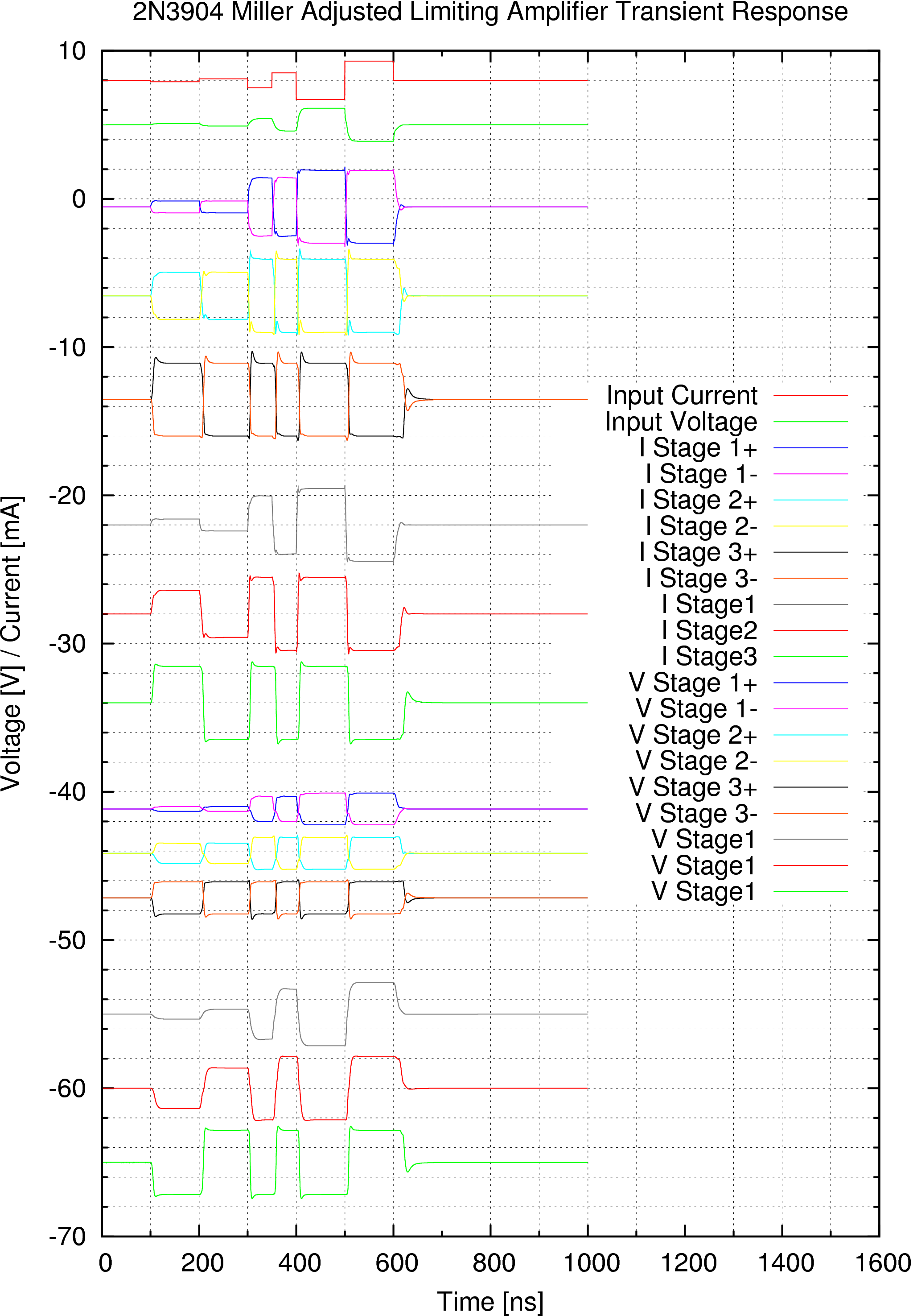
Miller Adjusted Cell Transient Response
|
|
To get a more accurate simulation I would have to replace the current sources
with real ones built from transistors.
|
|
|
The limiting amplifier works properly.
|
Number of stages necessary
We will have a 75 Ohm cable and a 75 Ohm output resistor. That gives
total loading of the last collector of 37.5 Ohm. On this I want to have 700mVpp.
That means 18mA current. Let's assume the whole receiver is made of 5mA limitter stages and we want
to have so many of them that the noise from the first one produces full range output.
Shot noise at 5mA and 16 MHz is 160nA. Amplification must be 101dB. With 12dB per
stage we need 8.4 stages to amplify and 1 to produce the shot noise. That
means 10 stages! With estimated 3 transistors 15 resistors and 8 capacitors per stage
that's 260 components and 550 pins to solder!
Let's try some better transistor that gives more decibels per stage.
I want a transistor that has higher Ft than 2N3904 (300 MHz) but not much
higher because then it's difficult to keep it from oscillating. I also want
cheap because there will be multiple stages lot of transistors. I looked at
Distrelec and they have BF199, 799, BFR 92P, 93AW, 182, 175 and BFS17P. GME has
BF199, 799, BFS17P. BF199 is very cheap and has SPICE model available from
NXP. Let's take BF199.

 Contact, support: Clock
on the Internet Relay Chat.© 1998-2016 Karel ‘Clock’ Kulhavý et al..
Contact, support: Clock
on the Internet Relay Chat.© 1998-2016 Karel ‘Clock’ Kulhavý et al.. 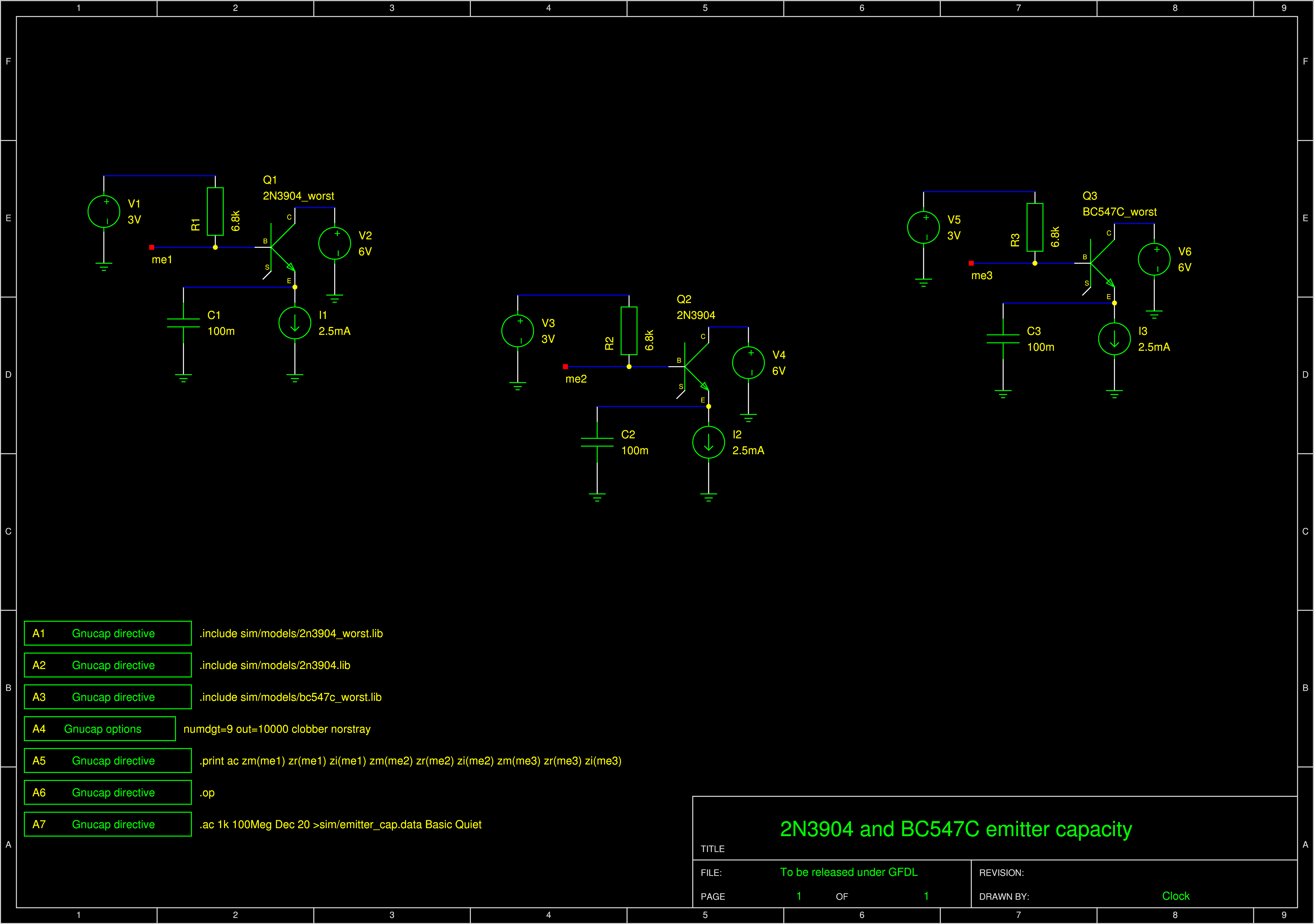


