 |
We are going to build PCB twister |
|
|
|
|
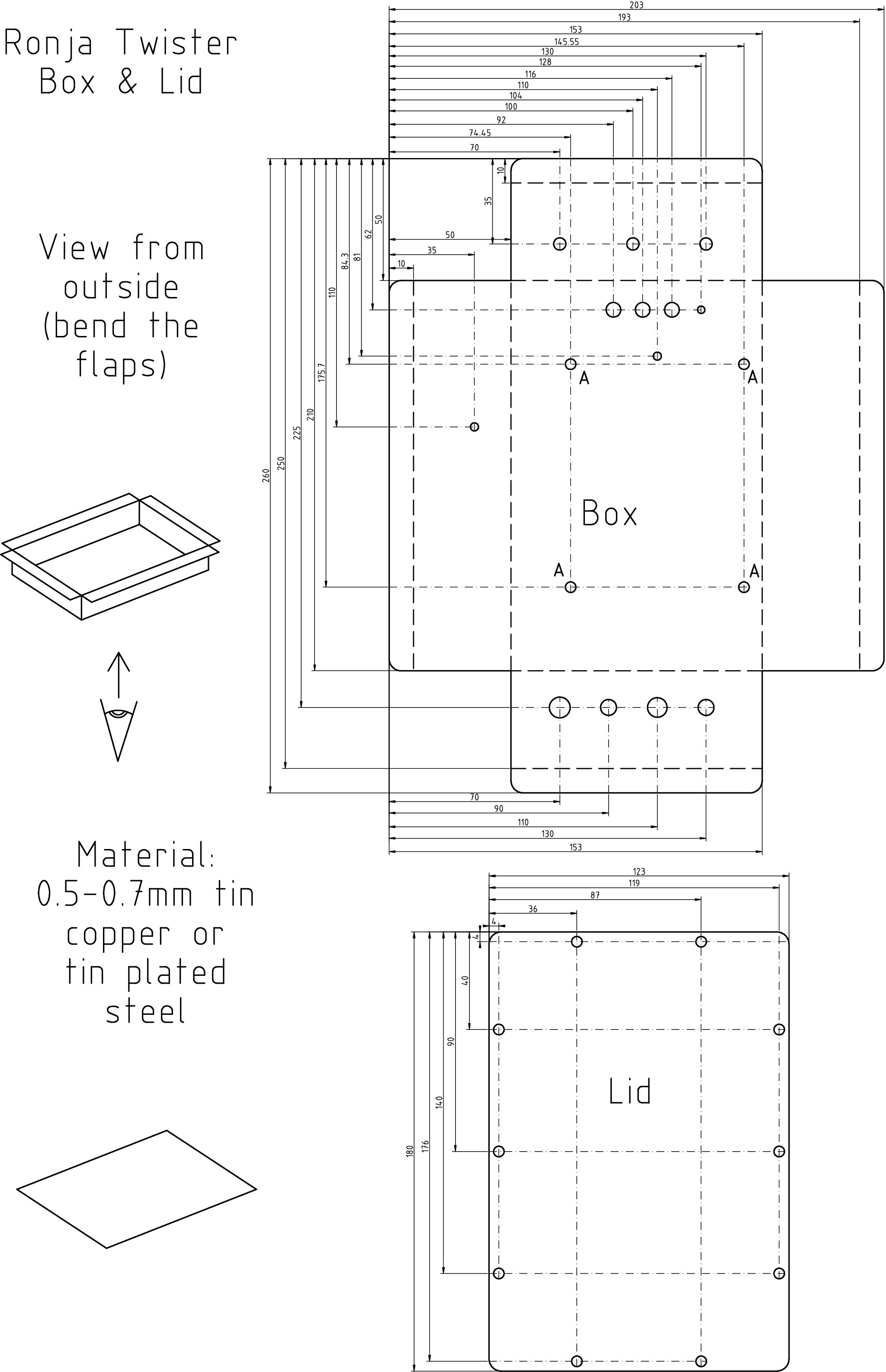
There are two possibilities how to make the box. First one is using
a
calibrated printer,
printing out a template and gluing the template on a tin.
The second one is measuring everything by hand. |
|
|
|
|
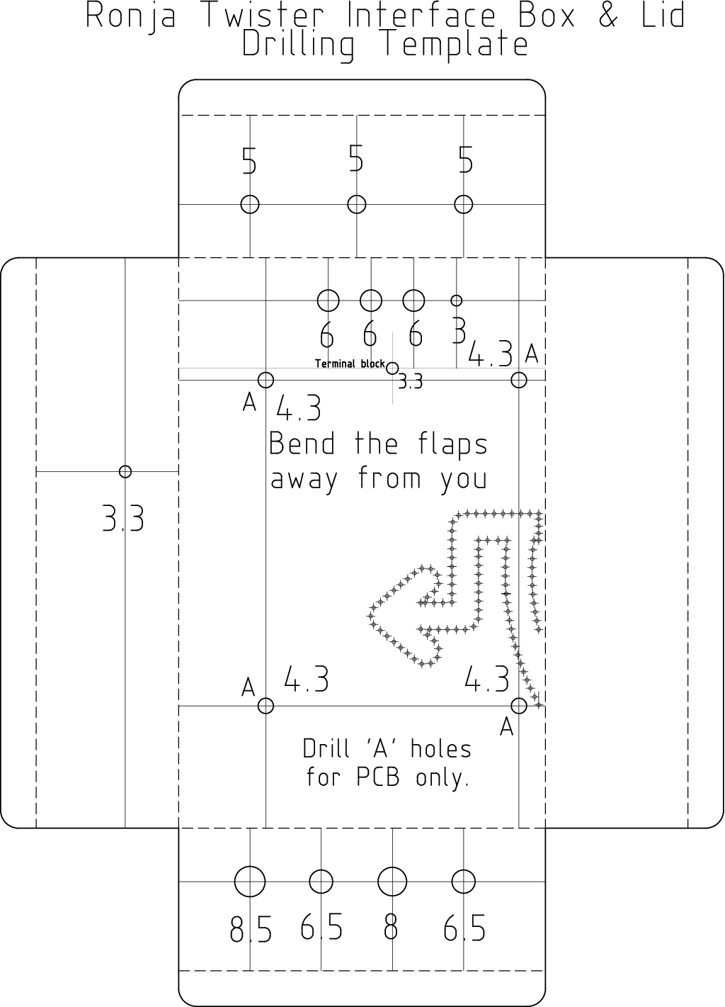
Option 1: Box body templatePrint out this template and glue on a piece of tin.
If you want not to install switches and use internal jumpers instead, strike
over the two 6.5mm holes. ![Gallery[edf]](http://images.twibright.com/tns/lvl0/edf.jpg)
|
|
|
|
|
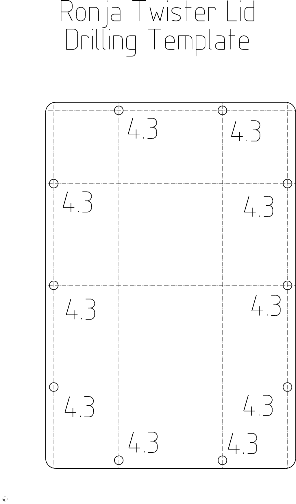
Option 1: Box lid templatePrint out this template and glue on a piece of tin. |
|
|
![Gallery[edd]](http://images.twibright.com/tns/lvl2/edd.jpg)
|
Option 1: Cutting outCut out the outline of the
templates. Use a pair of tin cutters. (Note: the photos are of obsolete template used on prototyping).
Tattoo the logo using a centre punch and hammer. Keep the strikes
consistent. ![Gallery[ede]](http://images.twibright.com/tns/lvl0/ede.jpg) |
|
|
|
|
Option 1: Drilling and bendingDrill out and bend
the box body and lid according to the print on the template, the plan and photos. Use the 20x20x3 steel L-sections fastened in a vice for bending. |
|
|
|
|
Option 2: making the box with manual measurementsMake the box according to the plan. Use hard stylus or thin nonporous surface marker for drawing lines. Use
square for maintaining perpendicularity and centre punch for making centres of
holes. Use the 20x20x3 steel L-sections fastened in a vice for bending the tin.
If you wish to use internal jumpers instead of external switches, do not drill
the two 6.5mm holes. |
|
|
![Gallery[ec6]](http://images.twibright.com/tns/lvl2/ec6.jpg)
|
Soldering cornersSolder corners up using
soldering iron, solder and rosin flux. If the box is made of copper, the soldering iron must be big and powerful or use two soldering irons (even they may
not suffice) or put the box on cooking stove, fire the cooking stove at appropriate power and perform the soldering on the stove. |
|
|
![Gallery[ec8]](http://images.twibright.com/tns/lvl2/ec8.jpg)
|
Lid holesMake holes on the box body by copying
them from the lid using a drill. Use 4.3mm drill bit. Use the bolts and
maybe nuts to secure the lid on already drilled holes during the operation.
Mark the lid so that you can put it back always the same way. Due to
drilling imperfections it may be difficult to close up the lid in some
other from the total 4 possible positions |
|
|
| Solder the wire into the 3mm hole. If the box is made of copper tin,
it is possible it will be impossible to solder with your soldering iron.
Either use a stronger soldering iron or two irons at once. If this is not
sufficient, place the box on a cooking stove and let the stove heat the
box and apply soldering iron on the hot box. |
|
![Gallery[ec9]](http://images.twibright.com/tns/lvl2/ec9.jpg)
|
GrommetssInstall one 6mm and three 4mm grommets.
(Note: The box on the picture is missing the hole for power connector.) |
|
|
![Gallery[eed]](http://images.twibright.com/tns/lvl2/eed.jpg)
|
Switches
Install switches. They have usually a lock against turning, use a tiny file
or a small drill to acoomodate the lock. |
|
|
![Gallery[1a3a]](http://images.twibright.com/tns/lvl2/1a3a.jpg)
|
Power connector
- Install power connector into the 8.5mm hole next to switches.
- Solder the outer contact to the box.
- Solder a 100nF capacitor (C114) between the inner contact and box.
|
|
|
|
|
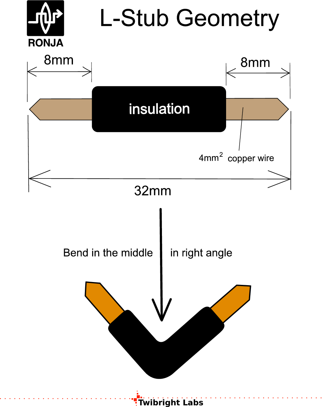
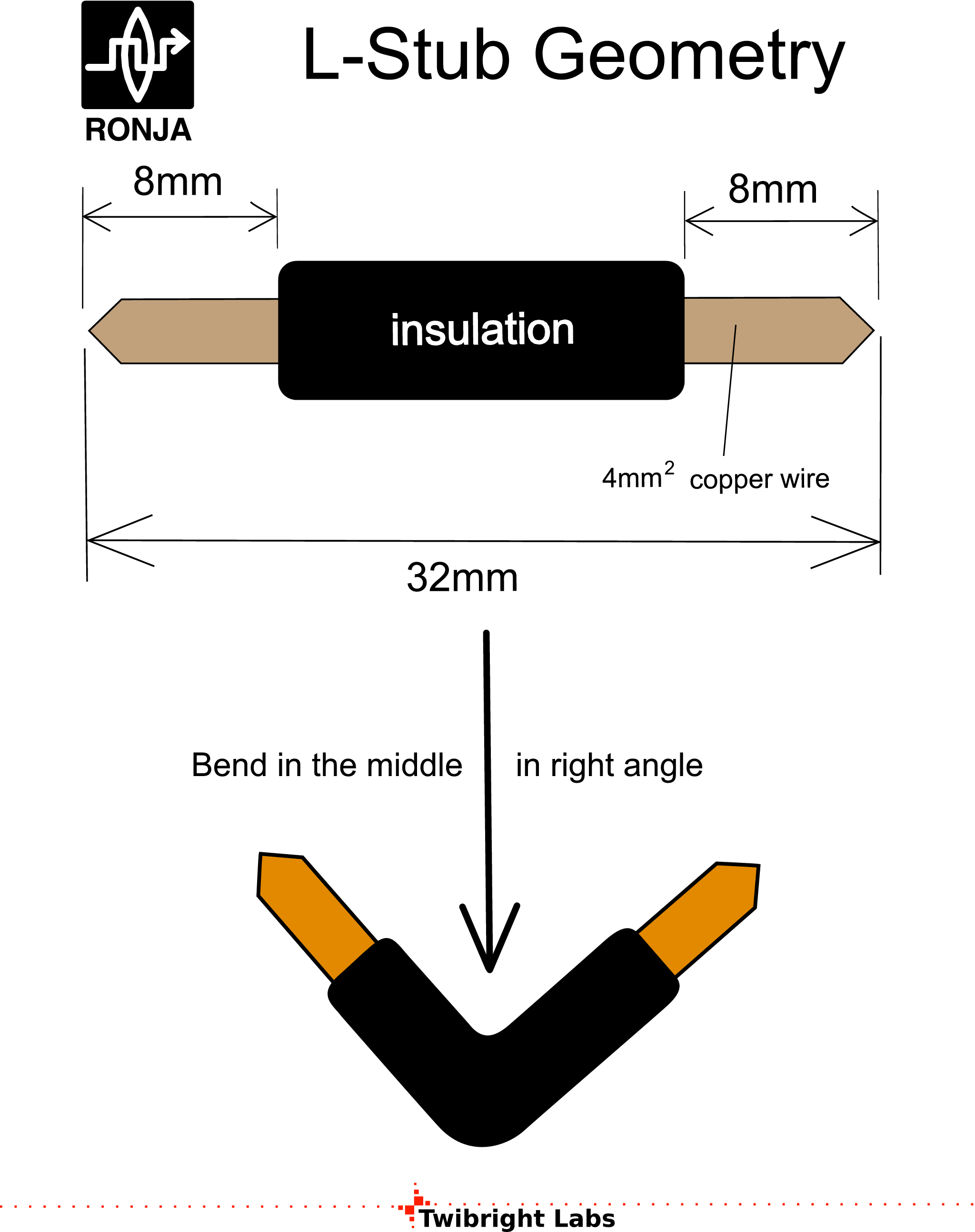
Making L stubs
Make 4 L-Stubs:
- 3 of them according to the picture
- 1 of them according to the picture but without the insulation
![Gallery[ed3]](http://images.twibright.com/tns/lvl1/ed3.jpg) |
|
|
![Gallery[ed3]](http://images.twibright.com/tns/lvl2/ed3.jpg)
|
Installing L Stubs
- Install 3 insulated wire stubs into the grommetss and 1 uninsulated into the
3mm hole next to the grommets to discriminate individual terminals of the
terminal block. The sidemost terminals are unused and prevent the terminal
block from breaking apart under mechanical stress from the cable.
- Solder C113 (100nF) on inner end of the L stub which
is most away from the uninsulated stub (rightmost on the picture EE5 below). Solder the other end of the capacitor
to the box.
![Gallery[ee5]](http://images.twibright.com/tns/lvl0/ee5.jpg) |
|
|
![Gallery[ecc]](http://images.twibright.com/tns/lvl2/ecc.jpg)
|
Mounting terminal blockMount the terminal
block. Wrench is 5.5mm.
Use M3x15 bolts and M3 washers and M3 nuts and tighten. |
|
|
![Gallery[ed6]](http://images.twibright.com/tns/lvl2/ed6.jpg)
|
Color bandsApply color bands with shown colors
made from duct tape. |
|
|
![Gallery[ed4]](http://images.twibright.com/tns/lvl2/ed4.jpg)
|
LEDsInsert LEDs into the box in the same
order as in the picture (from left: green, yellow, red). Glue them down using thermal glue pistol. |
|
|
![Gallery[ed8]](http://images.twibright.com/tns/lvl2/ed8.jpg)
|
STP cable
Cut 1m of the STP cable. Crimp a RJ-45 modular jack best with jacket at the end
(recommended wiring: T568B). Strip 50mm of outer insulation from the other (without jack) end of
the UTP cable. Strip 5mm from each individual wire. Put the cable through
it's grommet-equipped hole (the 6mm grommet in a group of four holes of varying
sizes). Adjust the length of unstripped cable between hole and stripped section
to 20mm. Fix up the cable in the hole using thermal glue. Seal from both sides,
using large amount of the glue. Note: the cable in the picture is not stranded, which
is wrong. |
|
|
Ribbon cable stubsCut the following pieces from stranded ribbon cables:
| Length | Number of wires in a cable | Number of cables (pieces) |
Note
| | 50mm | 2 | 3
| | 75mm | 4 | 1
| | 55mm | 3 | 1
| | 50mm | 6 | 2 | Omit if you wish to use internal jumpers
|
Separate all ends a bit and strip 4mm from all of them.
|
|
|
|
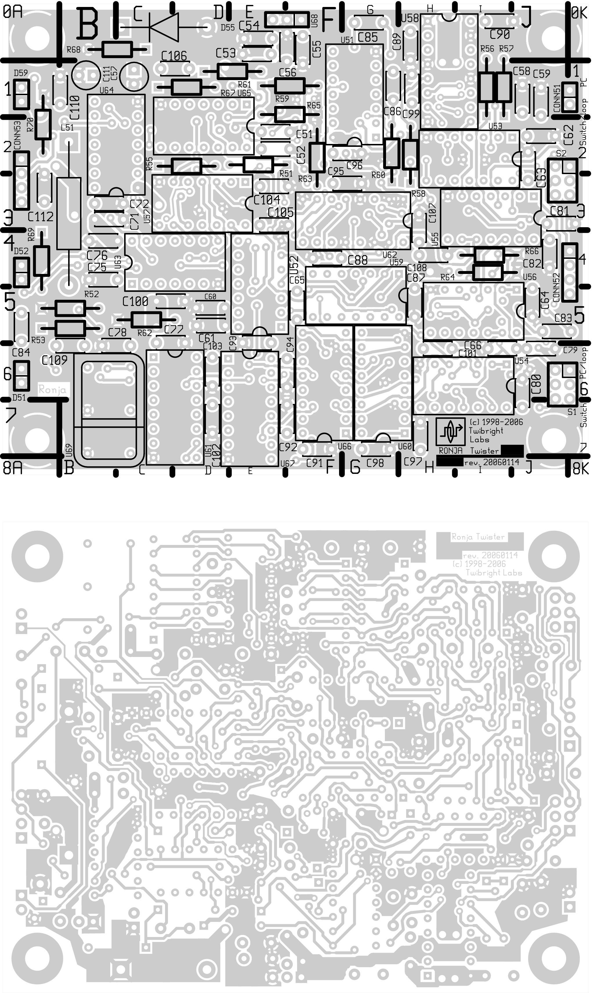
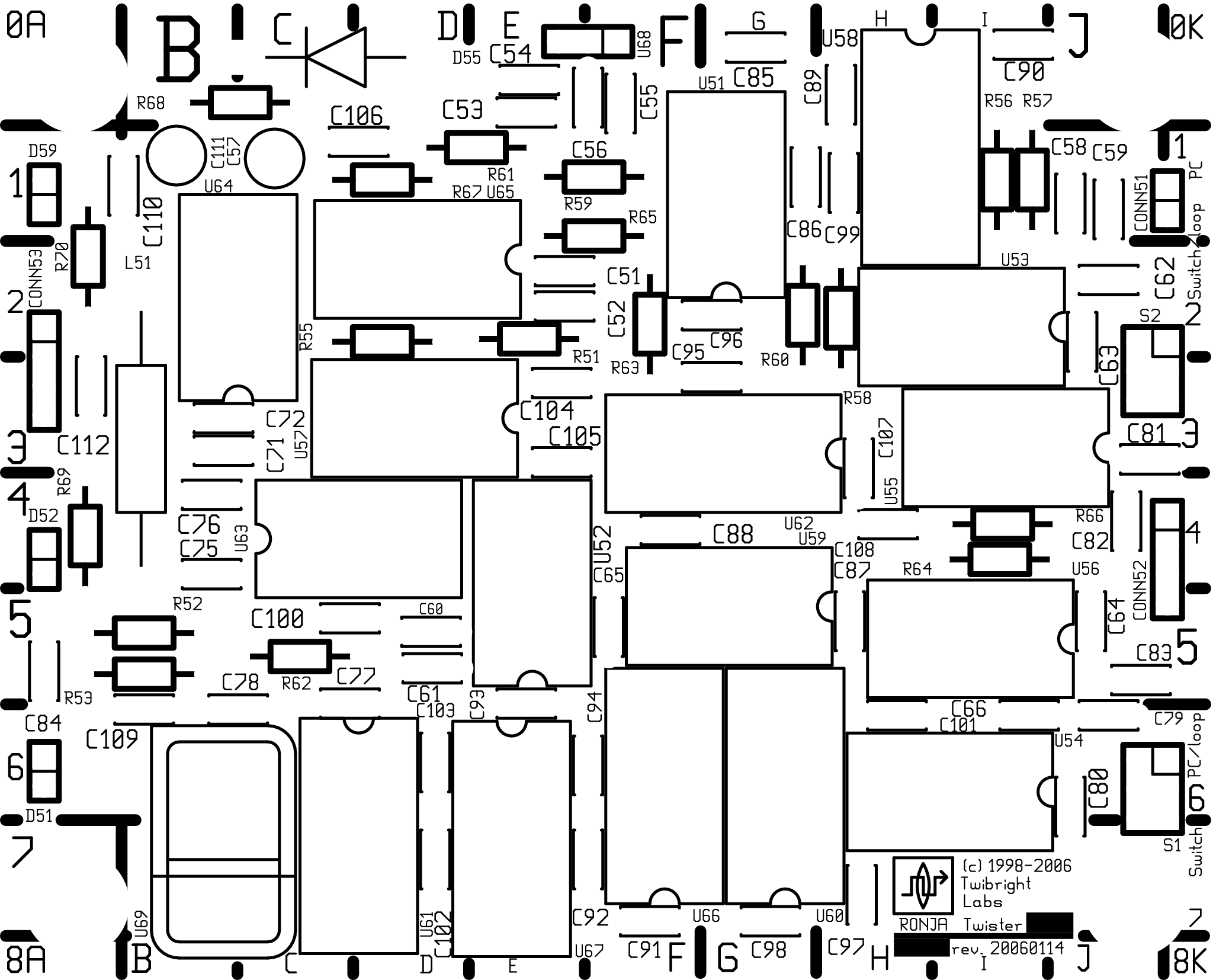
We are going to solder a PCB. All components will be stuck into
their holes according to silkscreen on the PCB and component reference table.
Their pins will be soldered using solder and rosin flux. A transformer
soldering iron (the one with the loop) or regulated-temperature iron is
used for this.
Keep the iron clean by periodical wiping. Use enough flux. The soldering of a joint should go this way: ensure there is enough solder and flux on the
iron, put the iron on the joint, wait 3 seconds. During these 3 seconds the solder
should automatically spread through the whole joint and make a neat cone.
If this doesn't happen, add solder or flux (because something of them
is missing, if the temperature of the iron is adequate at least a bit) and repeat. After the 3 seconds, remove the iron. |
|
|
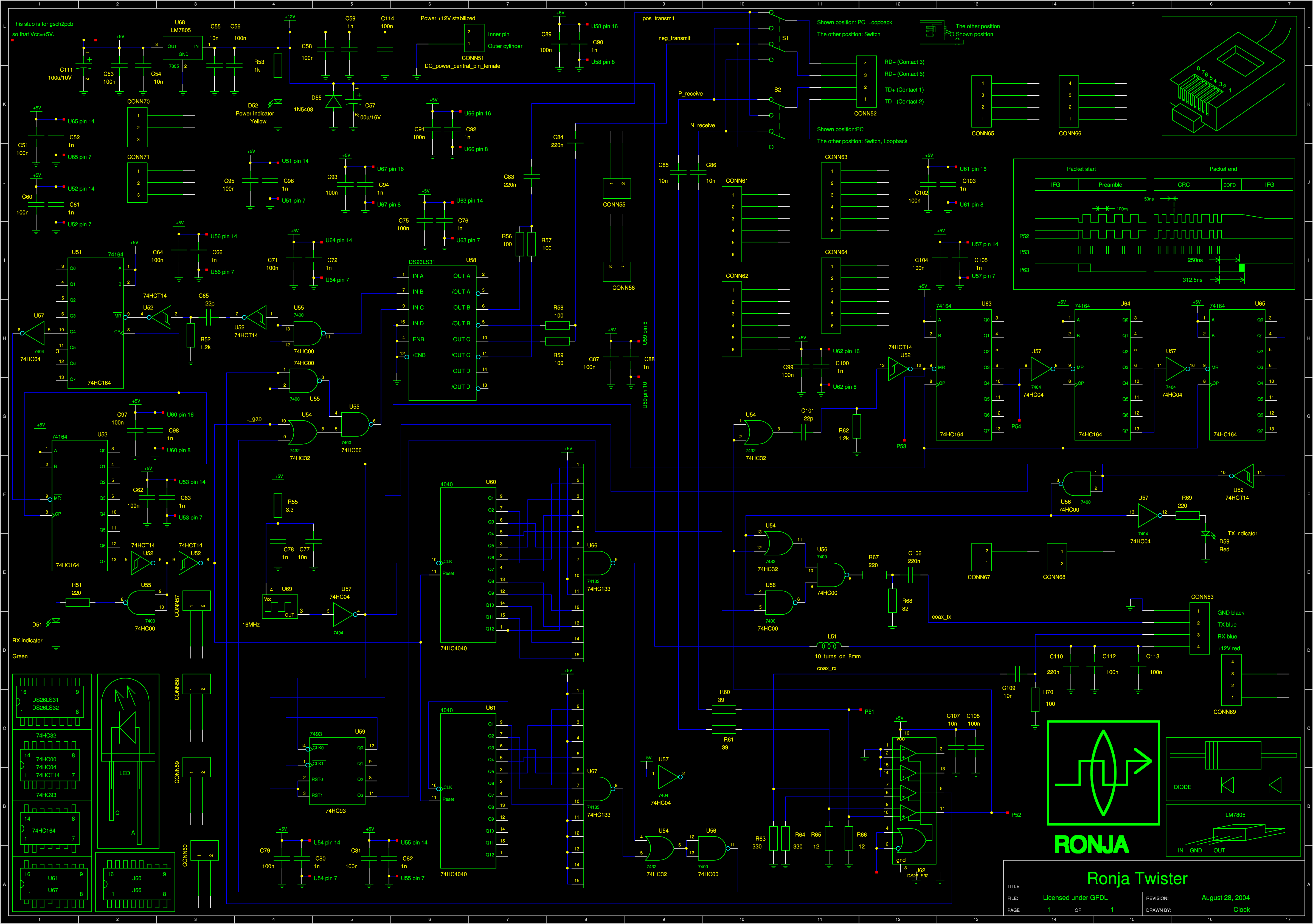
SchematicYou don't need the schematic, it's just for completeness here
|
|
|
|
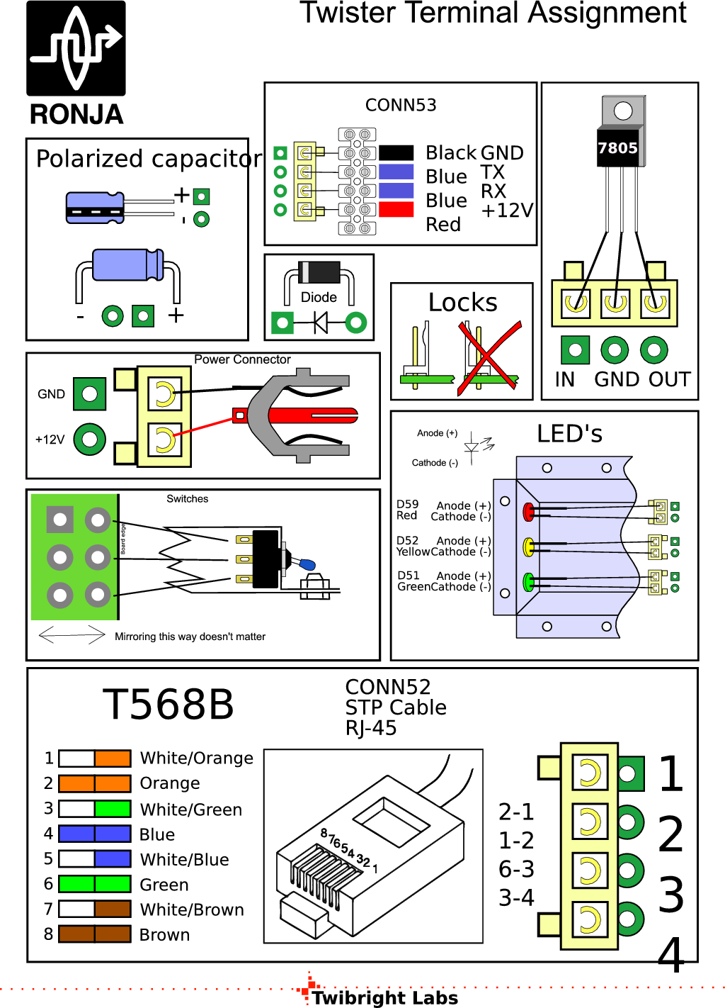
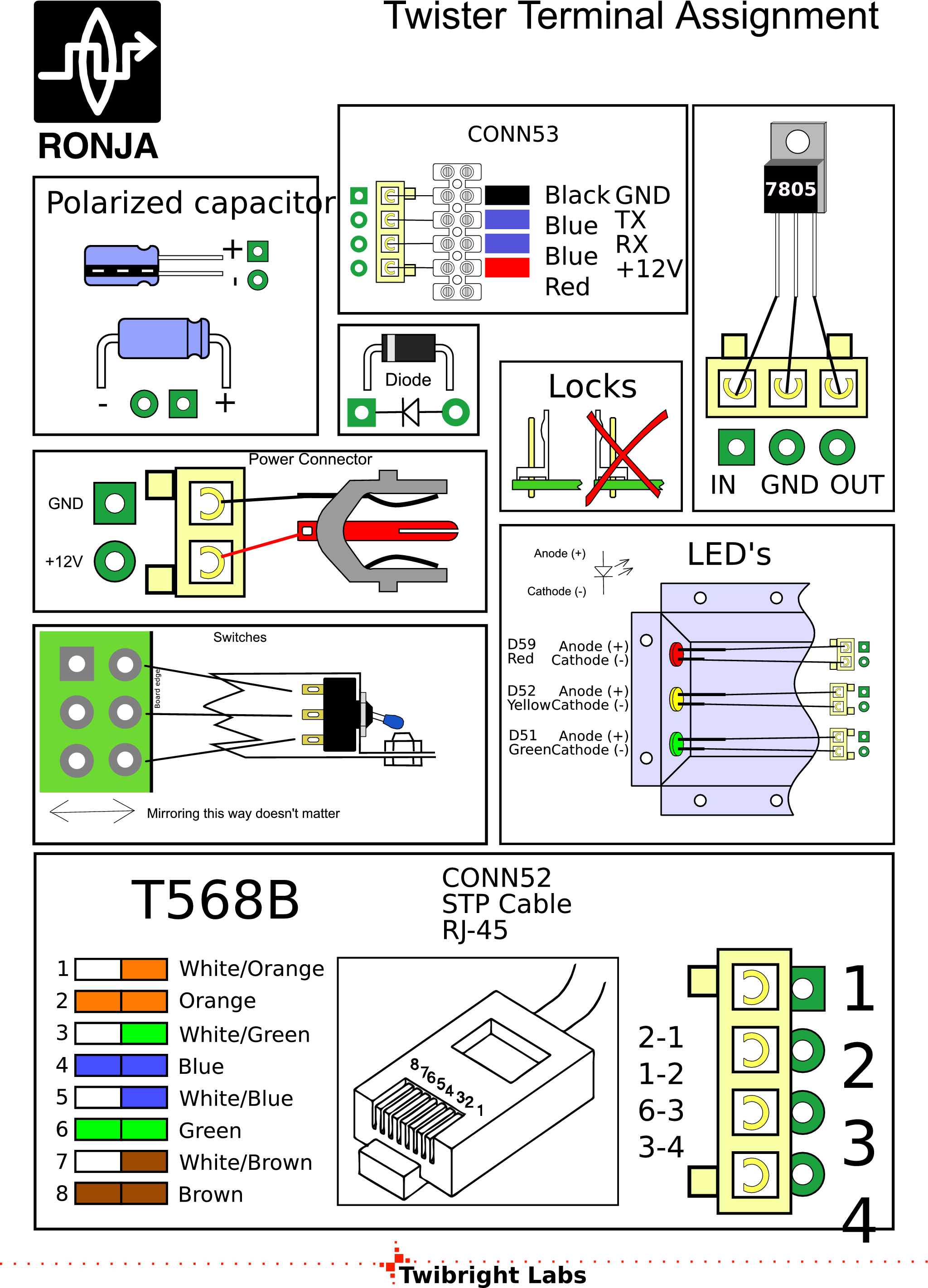
Assignment helper sheet
|
|
|
|
|
Print out the assembly picture. |
|
|
PartlistsThe partlists follow. They will be used during
population:
Single-part netlist
| Reference designator | Device | Value | Package | PCB Sector |
|---|
| C51 | CAPACITOR | 100n | ceramic 50V, rm 5mm | 2E |
| C52 | CAPACITOR | 1n | ceramic 50V, rm 5mm | 2E |
| C53 | CAPACITOR | 100n | ceramic 50V, rm 5mm | 0E |
| C54 | CAPACITOR | 10n | ceramic 50V, rm 5mm | 0E |
| C55 | CAPACITOR | 10n | ceramic 50V, rm 5mm | 0F |
| C56 | CAPACITOR | 100n | ceramic 50V, rm 5mm | 0F |
| C57 | POLARIZED_CAPACITOR | 100u/16V | miniature | 1C |
| C58 | CAPACITOR | 100n | ceramic 50V, rm 5mm | 1J |
| C59 | CAPACITOR | 1n | ceramic 50V, rm 5mm | 1J |
| C60 | CAPACITOR | 100n | ceramic 50V, rm 5mm | 5D |
| C61 | CAPACITOR | 1n | ceramic 50V, rm 5mm | 5D |
| C62 | CAPACITOR | 100n | ceramic 50V, rm 5mm | 2J |
| C63 | CAPACITOR | 1n | ceramic 50V, rm 5mm | 2J |
| C64 | CAPACITOR | 100n | ceramic 50V, rm 5mm | 5J |
| C65 | CAPACITOR | 22p | ceramic 50V, rm 5mm | 5F |
| C66 | CAPACITOR | 1n | ceramic 50V, rm 5mm | 6I |
| C71 | CAPACITOR | 100n | ceramic 50V, rm 5mm | 3B |
| C72 | CAPACITOR | 1n | ceramic 50V, rm 5mm | 3B |
| C75 | CAPACITOR | 100n | ceramic 50V, rm 5mm | 4B |
| C76 | CAPACITOR | 1n | ceramic 50V, rm 5mm | 4B |
| C77 | CAPACITOR | 10n | ceramic 50V, rm 5mm | 5C |
| C78 | CAPACITOR | 1n | ceramic 50V, rm 5mm | 6C |
| C79 | CAPACITOR | 100n | ceramic 50V, rm 5mm | 6J |
| C80 | CAPACITOR | 1n | ceramic 50V, rm 5mm | 6J |
| C81 | CAPACITOR | 100n | ceramic 50V, rm 5mm | 3J |
| C82 | CAPACITOR | 1n | ceramic 50V, rm 5mm | 4J |
| C83 | CAPACITOR | 220n | ceramic 50V, rm 5mm | 5J |
| C84 | CAPACITOR | 220n | ceramic 50V, rm 5mm | 5A |
| C85 | CAPACITOR | 10n | ceramic 50V, rm 5mm | 0G |
| C86 | CAPACITOR | 10n | ceramic 50V, rm 5mm | 1G |
| C87 | CAPACITOR | 100n | ceramic 50V, rm 5mm | 5H |
| C88 | CAPACITOR | 1n | ceramic 50V, rm 5mm | 4F |
| C89 | CAPACITOR | 100n | ceramic 50V, rm 5mm | 0H |
| C90 | CAPACITOR | 1n | ceramic 50V, rm 5mm | 0I |
| C91 | CAPACITOR | 100n | ceramic 50V, rm 5mm | 7F |
| C92 | CAPACITOR | 1n | ceramic 50V, rm 5mm | 7F |
| C93 | CAPACITOR | 100n | ceramic 50V, rm 5mm | 5E |
| C94 | CAPACITOR | 1n | ceramic 50V, rm 5mm | 6F |
| C95 | CAPACITOR | 100n | ceramic 50V, rm 5mm | 3G |
| C96 | CAPACITOR | 1n | ceramic 50V, rm 5mm | 2G |
| C97 | CAPACITOR | 100n | ceramic 50V, rm 5mm | 7H |
| C98 | CAPACITOR | 1n | ceramic 50V, rm 5mm | 7G |
| C99 | CAPACITOR | 100n | ceramic 50V, rm 5mm | 1H |
| C100 | CAPACITOR | 1n | ceramic 50V, rm 5mm | 5C |
| C101 | CAPACITOR | 22p | ceramic 50V, rm 5mm | 6H |
| C102 | CAPACITOR | 100n | ceramic 50V, rm 5mm | 7D |
| C103 | CAPACITOR | 1n | ceramic 50V, rm 5mm | 6D |
| C104 | CAPACITOR | 100n | ceramic 50V, rm 5mm | 3E |
| C105 | CAPACITOR | 1n | ceramic 50V, rm 5mm | 3E |
| C106 | CAPACITOR | 220n | ceramic 50V, rm 5mm | 1D |
| C107 | CAPACITOR | 10n | ceramic 50V, rm 5mm | 3H |
| C108 | CAPACITOR | 100n | ceramic 50V, rm 5mm | 4H |
| C109 | CAPACITOR | 10n | ceramic 50V, rm 5mm | 6B |
| C110 | CAPACITOR | 220n | ceramic 50V, rm 5mm | 1B |
| C111 | POLARIZED_CAPACITOR | 100u/10V | miniature | 1B |
| C112 | CAPACITOR | 100n | ceramic 50V, rm 5mm | 3A |
| C113 | CAPACITOR | 100n | ceramic 50V, rm 5mm | Not on PCB |
| C114 | CAPACITOR | 100n | ceramic 50V, rm 5mm | Not on PCB |
| CONN51 | DC_power_central_pin_female | 2.5mm | panel | 1K |
| CONN52 | HEADER_VERTICAL | 2.54mm 4-way 1-row | gold-plated with key | 4K |
| CONN53 | HEADER_VERTICAL | 2.54mm 4-way 1-row | gold-plated with key | 3A |
| CONN55 | HEADER_VERTICAL | 2.54mm 2-way | gold-plated with key | Not on PCB |
| CONN56 | HEADER_FEMALE | 2.54mm 2-way | gold-plated with key | Not on PCB |
| CONN57 | HEADER_VERTICAL | 2.54mm 2-way | gold-plated with key | Not on PCB |
| CONN58 | HEADER_VERTICAL | 2.54mm 2-way | gold-plated with key | Not on PCB |
| CONN59 | HEADER_FEMALE | 2.54mm 2-way | gold-plated with key | Not on PCB |
| CONN60 | HEADER_FEMALE | 2.54mm 2-way | gold-plated with key | Not on PCB |
| CONN61 | HEADER_VERTICAL | 2.54mm 6-way 2-row | gold-plated | Not on PCB |
| CONN62 | HEADER_VERTICAL | 2.54mm 6-way 2-row | gold-plated | Not on PCB |
| CONN63 | HEADER_FEMALE | 2.54mm 6-way 2-row | gold-plated | Not on PCB |
| CONN64 | HEADER_FEMALE | 2.54mm 6-way 2-row | gold-plated | Not on PCB |
| CONN65 | HEADER_FEMALE | 2.54mm 4-way 1-row | gold-plated with key | Not on PCB |
| CONN66 | RJ45 | | jack with jacket | Not on PCB |
| CONN67 | HEADER_VERTICAL | 2.54mm 2-way | gold-plated with key | Not on PCB |
| CONN68 | HEADER_FEMALE | 2.54mm 2-way | gold-plated with key | Not on PCB |
| CONN69 | HEADER_FEMALE | 2.54mm 4-way 1-row | gold-plated with key | Not on PCB |
| CONN70 | HEADER_VERTICAL | 2.54mm 3-way | gold-plated with key | Not on PCB |
| CONN71 | HEADER_FEMALE | 2.54mm 3-way | gold-plated with key | Not on PCB |
| D51 | LED | Green | 5mm diffuse | 6A |
| D52 | LED | Yellow | 5mm diffuse | 4A |
| D55 | 1N5408 | | | 0C |
| D59 | LED | Red | 5mm diffuse | 1A |
| L51 | COIL | 10_turns_on_8mm | custom | 3B |
| R51 | RESISTOR | 220 | 250mW pref. metallic | 2E |
| R52 | RESISTOR | 1.2k | 250mW pref. metallic | 5B |
| R53 | RESISTOR | 1k | 250mW pref. metallic | 5B |
| R55 | RESISTOR | 3.3 | 250mW pref. metallic | 2D |
| R56 | RESISTOR | 100 | 250mW pref. metallic | 1I |
| R57 | RESISTOR | 100 | 250mW pref. metallic | 1I |
| R58 | RESISTOR | 100 | 250mW pref. metallic | 2H |
| R59 | RESISTOR | 100 | 250mW pref. metallic | 1F |
| R60 | RESISTOR | 39 | 250mW pref. metallic | 2G |
| R61 | RESISTOR | 39 | 250mW pref. metallic | 1E |
| R62 | RESISTOR | 1.2k | 250mW pref. metallic | 5C |
| R63 | RESISTOR | 330 | 250mW pref. metallic | 2F |
| R64 | RESISTOR | 330 | 250mW pref. metallic | 4I |
| R65 | RESISTOR | 12 | 250mW pref. metallic | 1F |
| R66 | RESISTOR | 12 | 250mW pref. metallic | 4I |
| R67 | RESISTOR | 220 | 250mW pref. metallic | 1D |
| R68 | RESISTOR | 82 | 250mW pref. metallic | 0C |
| R69 | RESISTOR | 220 | 250mW pref. metallic | 4A |
| R70 | RESISTOR | 100 | 250mW pref. metallic | 2A |
| S1 | Switch DPDT ON-ON | gold-plated | 6mm hole | 6J |
| S2 | Switch DPDT ON-ON | gold-plated | 6mm hole | 3J |
| U51 | 74HC164 | | DIL | 1G |
| U52 | 74HCT14 | | DIL | 4E |
| U53 | 74HC164 | | DIL | 2I |
| U54 | 74HC32 | | DIL | 6I |
| U55 | 74HC00 | | DIL | 3I |
| U56 | 74HC00 | | DIL | 5I |
| U57 | 74HC04 | | DIL | 3D |
| U58 | DS26LS31 | | DIL | 1H |
| U59 | 74HC93 | | DIL | 5G |
| U60 | 74HC4040 | | DIL | 6G |
| U61 | 74HC4040 | | DIL | 7D |
| U62 | DS26LS32 | | DIL | 3G |
| U63 | 74HC164 | | DIL | 4D |
| U64 | 74HC164 | | DIL | 2C |
| U65 | 74HC164 | | DIL | 2D |
| U66 | 74HC133 | | DIL | 6F |
| U67 | 74HC133 | | DIL | 7E |
| U68 | LM7805 | | | 0F |
| U69 | CRYSTAL OSCILLATOR | 16MHz | DIL 14 | 7B |
Aggregated
partlist
| Device |
Package |
Value |
Quantity |
Reference designator -> PCB sector |
|---|
| 1N5408 | | | 1 |
|
| 74HC00 | DIL | | 2 |
|
| 74HC04 | DIL | | 1 |
|
| 74HC133 | DIL | | 2 |
|
| 74HC164 | DIL | | 5 |
- U51 -> 1G
- U53 -> 2I
- U63 -> 4D
- U64 -> 2C
- U65 -> 2D
|
| 74HC32 | DIL | | 1 |
|
| 74HC4040 | DIL | | 2 |
|
| 74HC93 | DIL | | 1 |
|
| 74HCT14 | DIL | | 1 |
|
| CAPACITOR | ceramic 50V, rm 5mm | 22p | 2 |
|
| CAPACITOR | ceramic 50V, rm 5mm | 1n | 19 |
- C100 -> 5C
- C103 -> 6D
- C105 -> 3E
- C52 -> 2E
- C59 -> 1J
- C61 -> 5D
- C63 -> 2J
- C66 -> 6I
- C72 -> 3B
- C76 -> 4B
- C78 -> 6C
- C80 -> 6J
- C82 -> 4J
- C88 -> 4F
- C90 -> 0I
- C92 -> 7F
- C94 -> 6F
- C96 -> 2G
- C98 -> 7G
|
| CAPACITOR | ceramic 50V, rm 5mm | 10n | 7 |
- C107 -> 3H
- C109 -> 6B
- C54 -> 0E
- C55 -> 0F
- C77 -> 5C
- C85 -> 0G
- C86 -> 1G
|
| CAPACITOR | ceramic 50V, rm 5mm | 100n | 24 |
- C102 -> 7D
- C104 -> 3E
- C108 -> 4H
- C112 -> 3A
- C113
- C114
- C51 -> 2E
- C53 -> 0E
- C56 -> 0F
- C58 -> 1J
- C60 -> 5D
- C62 -> 2J
- C64 -> 5J
- C71 -> 3B
- C75 -> 4B
- C79 -> 6J
- C81 -> 3J
- C87 -> 5H
- C89 -> 0H
- C91 -> 7F
- C93 -> 5E
- C95 -> 3G
- C97 -> 7H
- C99 -> 1H
|
| CAPACITOR | ceramic 50V, rm 5mm | 220n | 4 |
- C106 -> 1D
- C110 -> 1B
- C83 -> 5J
- C84 -> 5A
|
| COIL | custom | 10_turns_on_8mm | 1 |
|
| CRYSTAL OSCILLATOR | DIL 14 | 16MHz | 1 |
|
| DC_power_central_pin_female | panel | 2.5mm | 1 |
|
| DS26LS31 | DIL | | 1 |
|
| DS26LS32 | DIL | | 1 |
|
| HEADER_FEMALE | gold-plated | 2.54mm 6-way 2-row | 2 |
|
| HEADER_FEMALE | gold-plated with key | 2.54mm 2-way | 4 |
- CONN56
- CONN59
- CONN60
- CONN68
|
| HEADER_FEMALE | gold-plated with key | 2.54mm 3-way | 1 |
|
| HEADER_FEMALE | gold-plated with key | 2.54mm 4-way 1-row | 2 |
|
| HEADER_VERTICAL | gold-plated | 2.54mm 6-way 2-row | 2 |
|
| HEADER_VERTICAL | gold-plated with key | 2.54mm 2-way | 4 |
- CONN55
- CONN57
- CONN58
- CONN67
|
| HEADER_VERTICAL | gold-plated with key | 2.54mm 3-way | 1 |
|
| HEADER_VERTICAL | gold-plated with key | 2.54mm 4-way 1-row | 2 |
- CONN52 -> 4K
- CONN53 -> 3A
|
| LED | 5mm diffuse | Green | 1 |
|
| LED | 5mm diffuse | Red | 1 |
|
| LED | 5mm diffuse | Yellow | 1 |
|
| LM7805 | | | 1 |
|
| POLARIZED_CAPACITOR | miniature | 100u/10V | 1 |
|
| POLARIZED_CAPACITOR | miniature | 100u/16V | 1 |
|
| RESISTOR | 250mW pref. metallic | 3.3 | 1 |
|
| RESISTOR | 250mW pref. metallic | 12 | 2 |
|
| RESISTOR | 250mW pref. metallic | 39 | 2 |
|
| RESISTOR | 250mW pref. metallic | 82 | 1 |
|
| RESISTOR | 250mW pref. metallic | 100 | 5 |
- R56 -> 1I
- R57 -> 1I
- R58 -> 2H
- R59 -> 1F
- R70 -> 2A
|
| RESISTOR | 250mW pref. metallic | 220 | 3 |
- R51 -> 2E
- R67 -> 1D
- R69 -> 4A
|
| RESISTOR | 250mW pref. metallic | 330 | 2 |
|
| RESISTOR | 250mW pref. metallic | 1k | 1 |
|
| RESISTOR | 250mW pref. metallic | 1.2k | 2 |
|
| RJ45 | jack with jacket | | 1 |
|
| Switch DPDT ON-ON | 6mm hole | gold-plated | 2 |
|
|
|
|
|
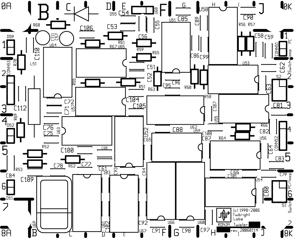
Sector marks
If you have revision 20051007 or earlier, you don't have sector
marks on the edges. Use a ruler and permanent marker to draw the marks by
1cm. |
|
|
![Gallery[ee0]](http://images.twibright.com/tns/lvl2/ee0.jpg)
|
SolderingSolder the parts into PCB in this order:
- IC sockets (if you are using them)
- Resistors
- Diodes
- All IC's except U68, if you are not using sockets
- Polarized capacitors
- Capacitors except C54, C55, C113, and C114
- CONN-designated connectors (51, 52, 53) with key oriented according to
assignment helper sheet
- instead of LEDs D51, D52, D59 solder the connectors called "Header vertical, pitch 2.54mm, gold plated, 1-row, 2-way, with key" with key oriented according to the assignment helper sheet
- On places S1, S2 solder the connectors called "Header socket, 2-row, 2.54mm pitch, 8.3mm depth, gold-plated, 6-way". You'll obtain them from "Header socket, 2-row, 2.54mm pitch, 8.3mm depth, gold-plated, 14-way" by cutting apart.
- Instead of U68, "Header vertical, pitch 2.54mm, gold plated, 1-row, 3-way, with key" according to assignment helper sheet
- Coil
|
|
|
![Gallery[fc5]](http://images.twibright.com/tns/lvl2/fc5.jpg)
|
If the revision of
PCB is 20040408 and earlier (check directly on the printed circuit board),
perform a bug fix according to the picture. Scratch out the green soldermask
on the adjacent plane and connect with pin as marked by red line.
The bug is harmless and has none or unnoticeable impact on
the performance of the device. If you are having other pieces of Twister with this bug already built into a case, do not bother with disassembly. Revision 20040807 has the bug already fixed. |
|
|
CleaningPour the isopropyl alcohol into the rectangular
pan and dip the PCB into it, components pointing upwards. Leave it there
for half an hour. Then brush all the rosin flux off with toothbrush, wash again
in the isopropyl alcohol, dip off and let dry up. |
|
|
|
Correctness checkTake the PCB and inspect it completely for:
- Left-out components (except C54, C55, C113, and C114)
- Correct values
- Correct IC
types
- Correct orientation of IC's
- Correct orientation of diodes.
- Correct orientation of polarized capacitors
- Correct orientation of
connector keys
- Joints soldered wrong or not at all
Printing this partlist and another copy of
assembly plan (left) will help for scratching out. |
|
|
 |
WarningWhat do you think would happen if you skip this correctness
check? "Your board would come to a screeching halt and you'd fly.
And you'd smash cement." -- Stacy Peralta, Dogtown and Z-Boys" |
|
|
|
|
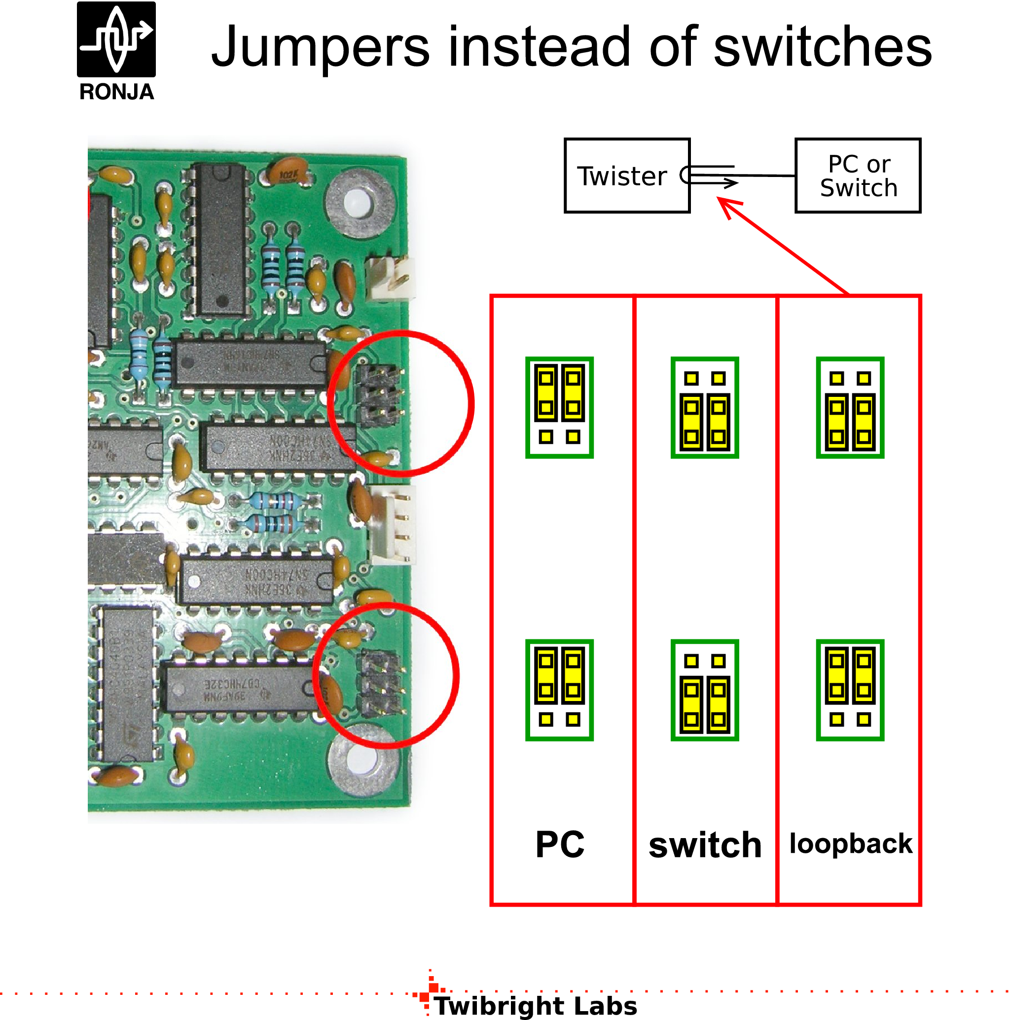
(Optional) jumpers
If you decided to use jumpers, jumper the board. |
|
|
|
|
Wiring connectorsAttach connectors
(except those for switches
if you decided to use internal jumpers instead) using the cable stubs from ribbon cable you
have already made. You can use insulating tube if you want to have it neater :)
Solder CONN52 connector the same way on the free end of the TP cable. Twist
the remaining 4 unused conductors together and solder them to the ground pin of
the power connector as seen in the photo, maybe using a piece of additional
wire. Keep this connection as short as possible so it also secures the cable
mechanically against pulling out. ![Gallery[ef6]](http://images.twibright.com/tns/lvl0/ef6.jpg)
|
|
|
|
|
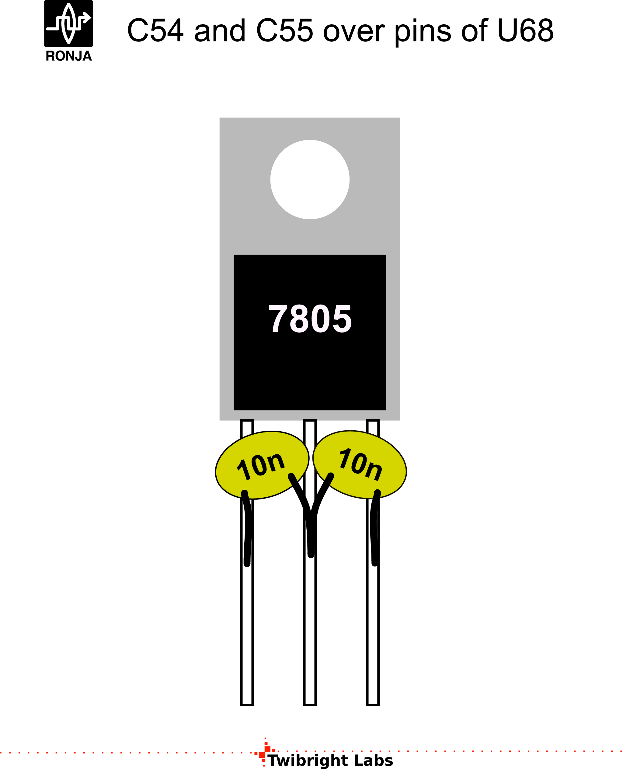
Regulator
Solder the C54 and C55 (both are the same value) directly on the
pins of U68. Mount U68 using one short M3 bolt, one M3 toothed spring washer
and one M3 nut onto it's hole from the inner side, it's pins pointing towards
the four big holes (connectors & switches).
|
|
|
![Gallery[ef6]](http://images.twibright.com/tns/lvl2/ef6.jpg)
|
Mounting boltsInsert the long M4 bolts into the
four holes for holding the PCB. Put a toothed spring washer on each one and
tighten up with M4 nut. Put another M4 nut and adjust the height of the nut so
that the distance between future PCB and the box will be 13mm. |
|
|
![Gallery[eb4]](http://images.twibright.com/tns/lvl2/eb4.jpg)
|
CompletionPut the PCB inside. Adjust the
M4 nuts so the PCB sits on 4 points and not only on 3. Put M4 washers
over it, M4 sprint washers, M4 nuts and tighten down. Put the lid
over and close with two bolts and save the remaining 8 nuts and 8 bolts.
The lid will be tightened down as soon as the Twister is tested. |
|
|
|
|
Labels
Print out the Twister label. Stick the label on the outer side of
the lid and fill in.
Print out the small schematic (see the Schematic section above)
and glue on the inner side of the lid. Cross over any component that is replaced
by an equivalent and inscribe the true equivalent type. |
|
|

 Contact, support: Clock
on the Internet Relay Chat.© 1998-2016 Karel ‘Clock’ Kulhavý et al..
Contact, support: Clock
on the Internet Relay Chat.© 1998-2016 Karel ‘Clock’ Kulhavý et al.. ![Gallery[eb4]](http://images.twibright.com/tns/lvl0/eb4.jpg)
![Gallery[ead]](http://images.twibright.com/tns/lvl0/ead.jpg)
![Gallery[ee0]](http://images.twibright.com/tns/lvl0/ee0.jpg)
![Gallery[ee1]](http://images.twibright.com/tns/lvl0/ee1.jpg)
![Gallery[eae]](http://images.twibright.com/tns/lvl0/eae.jpg)
![Gallery[eb5]](http://images.twibright.com/tns/lvl0/eb5.jpg)
![Gallery[eb6]](http://images.twibright.com/tns/lvl0/eb6.jpg)
![Gallery[eb7]](http://images.twibright.com/tns/lvl0/eb7.jpg)

![Gallery[ee7]](http://images.twibright.com/tns/lvl0/ee7.jpg)
![Gallery[eb9]](http://images.twibright.com/tns/lvl0/eb9.jpg)
![Gallery[ebc]](http://images.twibright.com/tns/lvl0/ebc.jpg)
![Gallery[ebd]](http://images.twibright.com/tns/lvl0/ebd.jpg)
![Gallery[ebe]](http://images.twibright.com/tns/lvl0/ebe.jpg)
![Gallery[ec0]](http://images.twibright.com/tns/lvl0/ec0.jpg)
![Gallery[ec1]](http://images.twibright.com/tns/lvl0/ec1.jpg)
![Gallery[ec2]](http://images.twibright.com/tns/lvl0/ec2.jpg)
![Gallery[ec3]](http://images.twibright.com/tns/lvl0/ec3.jpg)
![Gallery[ec4]](http://images.twibright.com/tns/lvl0/ec4.jpg)
![Gallery[eb8]](http://images.twibright.com/tns/lvl0/eb8.jpg)
![Gallery[eba]](http://images.twibright.com/tns/lvl0/eba.jpg)
![Gallery[ebb]](http://images.twibright.com/tns/lvl0/ebb.jpg)
![Gallery[ebf]](http://images.twibright.com/tns/lvl0/ebf.jpg)
![Gallery[ec5]](http://images.twibright.com/tns/lvl0/ec5.jpg)
![Gallery[ec7]](http://images.twibright.com/tns/lvl0/ec7.jpg)
![Gallery[eca]](http://images.twibright.com/tns/lvl0/eca.jpg)
![Gallery[ecb]](http://images.twibright.com/tns/lvl0/ecb.jpg)
![Gallery[ecc]](http://images.twibright.com/tns/lvl0/ecc.jpg)
![Gallery[ecd]](http://images.twibright.com/tns/lvl0/ecd.jpg)
![Gallery[ece]](http://images.twibright.com/tns/lvl0/ece.jpg)
![Gallery[ecf]](http://images.twibright.com/tns/lvl0/ecf.jpg)
![Gallery[ed0]](http://images.twibright.com/tns/lvl0/ed0.jpg)
![Gallery[ed1]](http://images.twibright.com/tns/lvl0/ed1.jpg)
![Gallery[ed2]](http://images.twibright.com/tns/lvl0/ed2.jpg)
![Gallery[eef]](http://images.twibright.com/tns/lvl0/eef.jpg)
![Gallery[ef0]](http://images.twibright.com/tns/lvl0/ef0.jpg)
![Gallery[ef1]](http://images.twibright.com/tns/lvl0/ef1.jpg)
![Gallery[ef3]](http://images.twibright.com/tns/lvl0/ef3.jpg)
![Gallery[ed7]](http://images.twibright.com/tns/lvl0/ed7.jpg)
![Gallery[ef2]](http://images.twibright.com/tns/lvl0/ef2.jpg)
![Gallery[ef4]](http://images.twibright.com/tns/lvl0/ef4.jpg)
![Gallery[ef5]](http://images.twibright.com/tns/lvl0/ef5.jpg)
![Gallery[f80]](http://images.twibright.com/tns/lvl0/f80.jpg)
![Gallery[f81]](http://images.twibright.com/tns/lvl0/f81.jpg)


